ATmega64A
7.6
Register Description
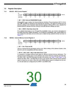
7.6.1
MCUCR – MCU Control Register
Bit
7
6
SRW10
R/W
0
5
SE
R/W
0
4
3
2
1
0
0x35 (0x55)
Read/Write
Initial Value
SRE
R/W
0
SM1
R/W
0
SM0
R/W
0
SM2
R/W
0
IVSEL
R/W
0
IVCE
R/W
0
MCUCR
• Bit 7 – SRE: External SRAM/XMEM Enable
Writing SRE to one enables the External Memory Interface.The pin functions AD7:0, A15:8,
ALE, WR, and RD are activated as the alternate pin functions. The SRE bit overrides any pin
direction settings in the respective data direction registers. Writing SRE to zero, disables the
External Memory Interface and the normal pin and data direction settings are used.
• Bit 6 – SRW10: Wait State Select Bit
For a detailed description in non ATmega103 compatibility mode, see common description for
the SRWn bits below (XMRA description). In ATmega103 compatibility mode, writing SRW10 to
one enables the wait state and one extra cycle is added during read/write strobe as shown in
Figure 7-7.
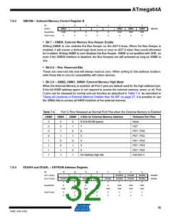
7.6.2
XMCRA – External Memory Control Register A
Bit
(0x6D)
7
6
5
4
SRL0
R/W
0
3
SRW01
R/W
0
2
SRW00
R/W
0
1
SRW11
R/W
0
0
–
–
SRL2
SRL1
R/W
0
XMCRA
Read/Write
Initial Value
R
0
R/W
0
R
0
• Bit 7 – Res: Reserved Bit
This is a reserved bit and will always read as zero. When writing to this address location, write
this bit to zero for compatibility with future devices.
• Bit 6:4 – SRL2, SRL1, SRL0: Wait State Sector Limit
It is possible to configure different wait states for different external memory addresses. The
external memory address space can be divided in two sectors that have separate wait-state bits.
The SRL2, SRL1, and SRL0 bits select the split of the sectors, see Table 7-2 and Figure 7-4. By
default, the SRL2, SRL1, and SRL0 bits are set to zero and the entire external memory address
space is treated as one sector. When the entire SRAM address space is configured as one sec-
tor, the wait states are configured by the SRW11 and SRW10 bits.
30
8160C–AVR–07/09

 ATMEL [ ATMEL ]