ATmega64A
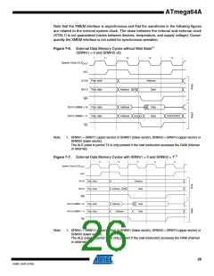
Note that the XMEM interface is asynchronous and that the waveforms in the following figures
are related to the internal system clock. The skew between the internal and external clock
(XTAL1) is not guaranteed (varies between devices, temperature, and supply voltage). Conse-
quently the XMEM interface is not suited for synchronous operation.
Figure 7-6. External Data Memory Cycles without Wait State(1)
(SRWn1 = 0 and SRWn0 =0)
T1
T2
T3
T4
System Clock (CLKCPU
)
ALE
A15:8 Prev. addr.
DA7:0 Prev. data
WR
Address
Data
Address
XX
DA7:0 (XMBK = 0) Prev. data
DA7:0 (XMBK = 1) Prev. data
RD
Address
Address
Data
Data
XXXXXXXX
XXXXX
Note:
1. SRWn1 = SRW11 (upper sector) or SRW01 (lower sector), SRWn0 = SRW10 (upper sector) or
SRW00 (lower sector).
The ALE pulse in period T4 is only present if the next instruction accesses the RAM (internal
or external).
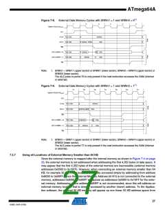
Figure 7-7. External Data Memory Cycles with SRWn1 = 0 and SRWn0 = 1(1)
T1
T2
T3
T4
T5
System Clock (CLKCPU
)
ALE
A15:8 Prev. Addr.
DA7:0 Prev. Data
WR
Address
Data
Address
Address
XX
DA7:0 (XMBK = 0) Prev. Data
DA7:0 (XMBK = 1) Prev. Data
RD
Data
Data
Address
Note:
1. SRWn1 = SRW11 (upper sector) or SRW01 (lower sector), SRWn0 = SRW10 (upper sector) or
SRW00 (lower sector).
The ALE pulse in period T5 is only present if the next instruction accesses the RAM (internal
or external).
26
8160C–AVR–07/09

 ATMEL [ ATMEL ]