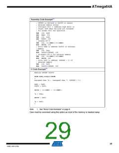
ATmega64A
• Bits 15:11 – Res: Reserved Bits
These are reserved bits and will always read as zero. When writing to this address location,
write these bits to zero for compatibility with future devices.
• Bits 10:0 – EEAR10:0: EEPROM Address
The EEPROM Address Registers – EEARH and EEARL specify the EEPROM address in the 2K
bytes EEPROM space. The EEPROM data bytes are addressed linearly between 0 and 2,048.
The Initial Value of EEAR is undefined. A proper value must be written before the EEPROM may
be accessed.
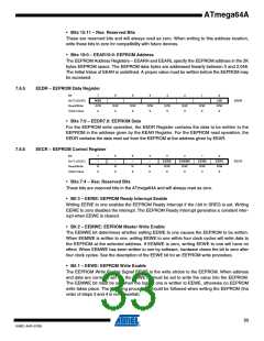
7.6.5
EEDR – EEPROM Data Register
Bit
0x1D (0x3D)
7
6
5
4
3
2
1
0
MSB
LSB
R/W
0
EEDR
Read/Write
Initial Value
R/W
0
R/W
0
R/W
0
R/W
0
R/W
0
R/W
0
R/W
0
• Bits 7:0 – EEDR7.0: EEPROM Data
For the EEPROM write operation, the EEDR Register contains the data to be written to the
EEPROM in the address given by the EEAR Register. For the EEPROM read operation, the
EEDR contains the data read out from the EEPROM at the address given by EEAR.
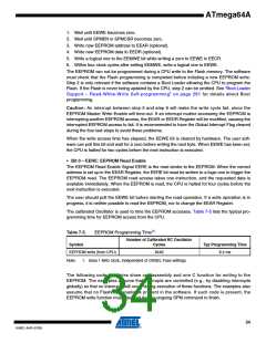
7.6.6
EECR – EEPROM Control Register
Bit
0x1C (0x3C)
7
6
–
5
–
4
–
3
EERIE
R/W
0
2
EEMWE
R/W
0
1
EEWE
R/W
X
0
EERE
R/W
0
–
EECR
Read/Write
Initial Value
R
0
R
0
R
0
R
0
• Bits 7:4 – Res: Reserved Bits
These bits are reserved bits in the ATmega64A and will always read as zero.
• Bit 3 – EERIE: EEPROM Ready Interrupt Enable
Writing EERIE to one enables the EEPROM Ready Interrupt if the I-bit in SREG is set. Writing
EERIE to zero disables the interrupt. The EEPROM Ready Interrupt generates a constant inter-
rupt when EEWE is cleared.
• Bit 2 – EEMWE: EEPROM Master Write Enable
The EEMWE bit determines whether setting EEWE to one causes the EEPROM to be written.
When EEMWE is written to one, writing EEWE to one within four clock cycles will write data to
the EEPROM at the selected address. If EEMWE is zero, writing EEWE to one will have no
effect. When EEMWE has been written to one by software, hardware clears the bit to zero after
four clock cycles. See the description of the EEWE bit for an EEPROM write procedure.
• Bit 1 – EEWE: EEPROM Write Enable
The EEPROM Write Enable Signal EEWE is the write strobe to the EEPROM. When address
and data are correctly set up, the EEWE bit must be set to write the value into the EEPROM.
The EEMWE bit must be set when the logical one is written to EEWE, otherwise no EEPROM
write takes place. The following procedure should be followed when writing the EEPROM (the
order of steps 3 and 4 is not essential):
33
8160C–AVR–07/09

 ATMEL [ ATMEL ]