ATmega64A
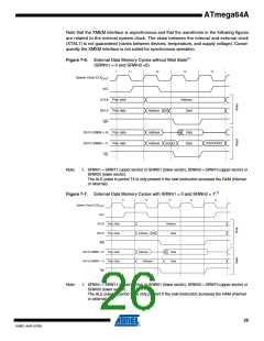
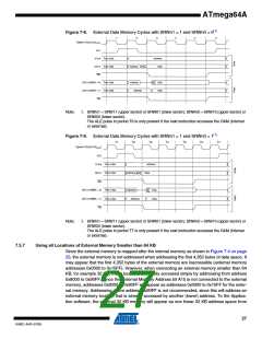
Figure 7-8. External Data Memory Cycles with SRWn1 = 1 and SRWn0 = 0(1)
T1
T2
T3
T4
T5
T6
System Clock (CLKCPU
)
ALE
A15:8 Prev. Addr.
DA7:0 Prev. Data
WR
Address
Data
Address
Address
XX
DA7:0 (XMBK = 0) Prev. Data
DA7:0 (XMBK = 1) Prev. Data
RD
Data
Data
Address
Note:
1. SRWn1 = SRW11 (upper sector) or SRW01 (lower sector), SRWn0 = SRW10 (upper sector) or
SRW00 (lower sector).
The ALE pulse in period T6 is only present if the next instruction accesses the RAM (internal
or external).
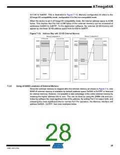
Figure 7-9. External Data Memory Cycles with SRWn1 = 1 and SRWn0 = 1(1)
T1
T2
T3
T4
T5
T6
T7
System Clock (CLKCPU
)
ALE
A15:8 Prev. Addr.
DA7:0 Prev. Data
WR
Address
Address XX
Data
DA7:0 (XMBK = 0) Prev. Data
DA7:0 (XMBK = 1) Prev. Data
RD
Address
Address
Data
Data
Note:
1. SRWn1 = SRW11 (upper sector) or SRW01 (lower sector), SRWn0 = SRW10 (upper sector) or
SRW00 (lower sector).
The ALE pulse in period T7 is only present if the next instruction accesses the RAM (internal
or external).
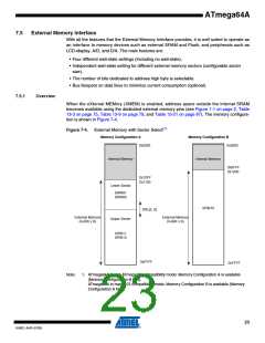
7.5.7
Using all Locations of External Memory Smaller than 64 KB
Since the external memory is mapped after the internal memory as shown in Figure 7-4 on page
23, the external memory is not addressed when addressing the first 4,352 bytes of data space. It
may appear that the first 4,352 bytes of the external memory are inaccessible (external memory
addresses 0x0000 to 0x10FF). However, when connecting an external memory smaller than 64
KB, for example 32 KB, these locations are easily accessed simply by addressing from address
0x8000 to 0x90FF. Since the External Memory Address bit A15 is not connected to the external
memory, addresses 0x8000 to 0x90FF will appear as addresses 0x0000 to 0x10FF for the exter-
nal memory. Addressing above address 0x90FF is not recommended, since this will address an
external memory location that is already accessed by another (lower) address. To the Applica-
tion software, the external 32 KB memory will appear as one linear 32 KB address space from
27
8160C–AVR–07/09

 ATMEL [ ATMEL ]