ATmega64A
• D to Q propagation delay (tpd).
• Data setup time before G low (tsu).
• Data (address) hold time after G low (th).
The external memory interface is designed to guaranty minimum address hold time after G is
asserted low of th = 5 ns (refer to tLAXX_LD/tLLAXX_ST in Table 28-8 to Table 28-15 on page 340).
The D to Q propagation delay (tpd) must be taken into consideration when calculating the access
time requirement of the external component. The data setup time before G low (tsu) must not
exceed address valid to ALE low (tAVLLC) minus PCB wiring delay (dependent on the capacitive
load).
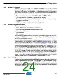
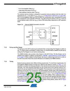
Figure 7-5. External SRAM Connected to the AVR
D[7:0]
AD7:0
ALE
D
G
Q
A[7:0]
SRAM
A[15:8]
AVR
A15:8
RD
RD
WR
WR
7.5.5
Pull-up and Bus Keeper
The pull-ups on the AD7:0 ports may be activated if the corresponding Port Register is written to
one. To reduce power consumption in sleep mode, it is recommended to disable the pull-ups by
writing the Port Register to zero before entering sleep.
The XMEM interface also provides a Bus Keeper on the AD7:0 lines. The Bus Keeper can be
disabled and enabled in software as described in “XMCRB – External Memory Control Register
B” on page 32. When enabled, the Bus Keeper will ensure a defined logic level (zero or one) on
the AD7:0 bus when these lines would otherwise be tri-stated by the XMEM interface.
7.5.6
Timing
External memory devices have different timing requirements. To meet these requirements, the
ATmega64A XMEM interface provides four different wait states as shown in Table 7-3. It is
important to consider the timing specification of the external memory device before selecting the
wait-state. The most important parameters are the access time for the external memory com-
pared to the set-up requirement of the ATmega64A. The access time for the external memory is
defined to be the time from receiving the chip select/address until the data of this address actu-
ally is driven on the bus. The access time cannot exceed the time from the ALE pulse is asserted
low until data must be stable during a read sequence (tLLRL+ tRLRH - tDVRH in Table 28-8 to Table
28-15 on page 340). The different wait states are set up in software. As an additional feature, it
is possible to divide the external memory space in two sectors with individual wait-state settings.
This makes it possible to connect two different memory devices with different timing require-
ments to the same XMEM interface. For XMEM interface timing details, please refer to Figure
28-6 to Figure 28-9, and Table 28-8 to Table 28-15.
25
8160C–AVR–07/09

 ATMEL [ ATMEL ]