ATmega64A
7.5.2
ATmega103 Compatibility
Both External Memory Control Registers, XMCRA and XMCRB, are placed in Extended I/O
space. In ATmega103 compatibility mode, these registers are not available, and the features
selected by these registers are not available. The device is still ATmega103 compatible, as
these features did not exist in ATmega103. The limitations in ATmega103 compatibility mode
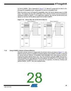
are:
• Only two wait-state settings are available (SRW1n = 0b00 and SRW1n = 0b01).
• The number of bits that are assigned to address high byte are fixed.
• The external memory section cannot be divided into sectors with different wait-state settings.
• Bus Keeper is not available.
• RD, WR, and ALE pins are output only (Port G in ATmega64A).
7.5.3
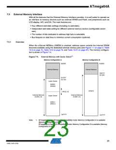
Using the External Memory Interface
The interface consists of:
• AD7:0: Multiplexed low-order address bus and data bus.
• A15:8: High-order address bus (configurable number of bits).
• ALE: Address latch enable.
• RD: Read strobe.
• WR: Write strobe.
The control bits for the External Memory Interface are located in three registers, the MCU Con-
trol Register – MCUCR, the External Memory Control Register A – XMCRA, and the External
Memory Control Register B – XMCRB.
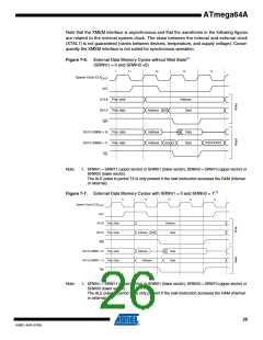
When the XMEM interface is enabled, the XMEM interface will override the setting in the Data
Direction Registers that corresponds to the ports dedicated to the XMEM interface. For details
about the port override, see the alternate functions in section “I/O Ports” on page 68. The XMEM
interface will auto-detect whether an access is internal or external. If the access is external, the
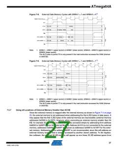
XMEM interface will output address, data, and the control signals on the ports according to Fig-
ure 7-6 (this figure shows the wave forms without wait states). When ALE goes from high-to-low,
there is a valid address on AD7:0. ALE is low during a data transfer. When the XMEM interface
is enabled, also an internal access will cause activity on address-, data- and ALE ports, but the
RD and WR strobes will not toggle during internal access. When the external memory interface
is disabled, the normal pin and data direction settings are used. Note that when the XMEM inter-
face is disabled, the address space above the internal SRAM boundary is not mapped into the
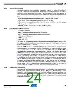
internal SRAM. Figure 7-5 illustrates how to connect an external SRAM to the AVR using an
octal latch (typically 74 x 573 or equivalent) which is transparent when G is high.
7.5.4
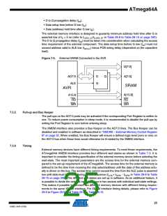
Address Latch Requirements
Due to the high-speed operation of the XRAM interface, the address latch must be selected with
care for system frequencies above 8 MHz @ 4V and 4 MHz @ 2.7V. When operating at condi-
tions above these frequencies, the typical old style 74HC series latch becomes inadequate. The
external memory interface is designed in compliance to the 74AHC series latch. However, most
latches can be used as long they comply with the main timing parameters. The main parameters
for the address latch are:
24
8160C–AVR–07/09

 ATMEL [ ATMEL ]