ATmega64A
as a consequence, the device does not enter Power-down entirely. It is therefore recommended
to verify that the EEPROM write operation is completed before entering Power-down.
7.3.3
Preventing EEPROM Corruption
During periods of low VCC, the EEPROM data can be corrupted because the supply voltage is
too low for the CPU and the EEPROM to operate properly. These issues are the same as for
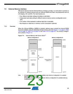
board level systems using EEPROM, and the same design solutions should be applied.
An EEPROM data corruption can be caused by two situations when the voltage is too low. First,
a regular write sequence to the EEPROM requires a minimum voltage to operate correctly. Sec-
ondly, the CPU itself can execute instructions incorrectly, if the supply voltage is too low.
EEPROM data corruption can easily be avoided by following this design recommendation:
Keep the AVR RESET active (low) during periods of insufficient power supply voltage. This can
be done by enabling the internal Brown-out Detector (BOD). If the detection level of the internal
BOD does not match the needed detection level, an external low VCC Reset Protection circuit
can be used. If a reset occurs while a write operation is in progress, the write operation will be
completed provided that the power supply voltage is sufficient.
7.4
I/O Memory
The I/O space definition of the ATmega64A is shown in “Register Summary” on page 373.
All ATmega64A I/Os and peripherals are placed in the I/O space. All I/O locations may be
accessed by the LD/LDS/LDD and ST/STS/STD instructions, transferring data between the 32
general purpose working registers and the I/O space. I/O Registers within the address range
0x00 - 0x1F are directly bit-accessible using the SBI and CBI instructions. In these registers, the
value of single bits can be checked by using the SBIS and SBIC instructions. Refer to the
instruction set section for more details. When using the I/O specific commands IN and OUT, the
I/O addresses 0x00 - 0x3F must be used. When addressing I/O Registers as data space using
LD and ST instructions, 0x20 must be added to these addresses. The ATmega64A is a complex
microcontroller with more peripheral units than can be supported within the 64 location reserved
in Opcode for the IN and OUT instructions. For the Extended I/O space from 0x60 - 0xFF in
SRAM, only the ST/STS/STD and LD/LDS/LDD instructions can be used. The Extended I/O
space is replaced with SRAM locations when the ATmega64A is in the ATmega103 compatibility
mode.
For compatibility with future devices, reserved bits should be written to zero if accessed.
Reserved I/O memory addresses should never be written.
Some of the status flags are cleared by writing a logical one to them. Note that the CBI and SBI
instructions will operate on all bits in the I/O Register, writing a one back into any flag read as
set, thus clearing the flag. The CBI and SBI instructions work with registers 0x00 to 0x1F only.
The I/O and peripherals control registers are explained in later sections.
22
8160C–AVR–07/09

 ATMEL [ ATMEL ]