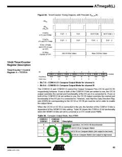
ATmega8(L)
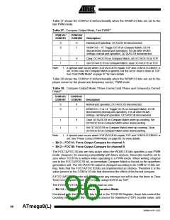
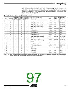
to 3. See Table 38 on page 96. The actual OC1x value will only be visible on the port pin
if the data direction for the port pin is set as output (DDR_OC1x). The PWM waveform is
generated by setting (or clearing) the OC1x Register at the Compare Match between
OCR1x and TCNT1 when the counter increments, and clearing (or setting) the OC1x
Register at Compare Match between OCR1x and TCNT1 when the counter decrements.
The PWM frequency for the output when using phase and frequency correct PWM can
be calculated by the following equation:
f
clk_I/O
f
= ---------------------------
OCnxPFCPWM
2 N TOP
The N variable represents the prescaler divider (1, 8, 64, 256, or 1024).
The extreme values for the OCR1x Register represents special cases when generating
a PWM waveform output in the phase correct PWM mode. If the OCR1x is set equal to
BOTTOM the output will be continuously low and if set equal to TOP the output will be
set to high for non-inverted PWM mode. For inverted PWM the output will have the
opposite logic values.
If OCR1A is used to define the TOP value (WGM13:0 = 9) and COM1A1:0 = 1, the
OC1A output will toggle with a 50% duty cycle.
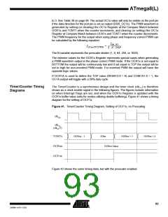
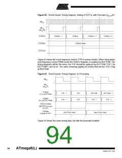
Timer/Counter Timing
Diagrams
The Timer/Counter is a synchronous design and the timer clock (clkT1) is therefore
shown as a clock enable signal in the following figures. The figures include information
on when Interrupt Flags are set, and when the OCR1x Register is updated with the
OCR1x buffer value (only for modes utilizing double buffering). Figure 41 shows a timing
diagram for the setting of OCF1x.
Figure 41. Timer/Counter Timing Diagram, Setting of OCF1x, no Prescaling
clkI/O
clkTn
(clkI/O/1)
TCNTn
OCRnx
OCFnx
OCRnx - 1
OCRnx
OCRnx + 1
OCRnx + 2
OCRnx Value
Figure 42 shows the same timing data, but with the prescaler enabled.
93
2486M–AVR–12/03

 ATMEL [ ATMEL ]