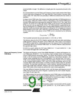
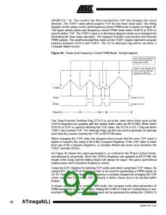
ATmega8(L)
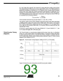
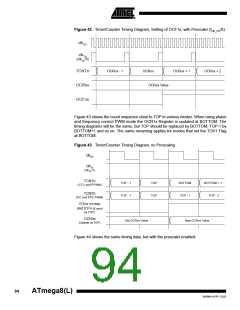
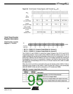
Figure 44. Timer/Counter Timing Diagram, with Prescaler (fclk_I/O/8)
clkI/O
clkTn
(clkI/O/8)
TCNTn
TOP - 1
TOP - 1
TOP
TOP
BOTTOM
TOP - 1
BOTTOM + 1
TOP - 2
(CTC and FPWM)
TCNTn
(PC and PFC PWM)
TOVn (FPWM)
and ICFn (if used
as TOP)
OCRnx
(Update at TOP)
Old OCRnx Value
New OCRnx Value
16-bit Timer/Counter
Register Description
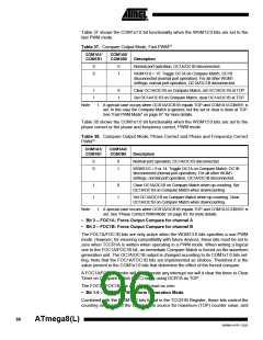
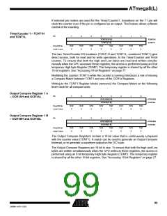
Timer/Counter 1 Control
Register A – TCCR1A
Bit
7
COM1A1
R/W
6
5
COM1B1
R/W
4
3
FOC1A
W
2
FOC1B
W
1
WGM11
R/W
0
0
WGM10
R/W
0
COM1A0
R/W
0
COM1B0
R/W
0
TCCR1A
Read/Write
Initial Value
0
0
0
0
• Bit 7:6 – COM1A1:0: Compare Output Mode for channel A
• Bit 5:4 – COM1B1:0: Compare Output Mode for channel B
The COM1A1:0 and COM1B1:0 control the Output Compare Pins (OC1A and OC1B
respectively) behavior. If one or both of the COM1A1:0 bits are written to one, the OC1A
output overrides the normal port functionality of the I/O pin it is connected to. If one or
both of the COM1B1:0 bit are written to one, the OC1B output overrides the normal port
functionality of the I/O pin it is connected to. However, note that the Data Direction Reg-
ister (DDR) bit corresponding to the OC1A or OC1B pin must be set in order to enable
the output driver.
When the OC1A or OC1B is connected to the pin, the function of the COM1x1:0 bits is
dependent of the WGM13:0 bits setting. Table 36 shows the COM1x1:0 bit functionality
when the WGM13:0 bits are set to a normal or a CTC mode (non-PWM).
Table 36. Compare Output Mode, Non-PWM
COM1A1/
COM1B1
COM1A0/
COM1B0
Description
0
0
1
1
0
1
0
1
Normal port operation, OC1A/OC1B disconnected.
Toggle OC1A/OC1B on Compare Match
Clear OC1A/OC1B on Compare Match (Set output to low level)
Set OC1A/OC1B on Compare Match (Set output to high level)
95
2486M–AVR–12/03

 ATMEL [ ATMEL ]