ATmega8(L)
ing at 0x0000 before the Compare Match can occur. The OCR1A Register, however, is
double buffered. This feature allows the OCR1A I/O location to be written anytime.
When the OCR1A I/O location is written the value written will be put into the OCR1A
Buffer Register. The OCR1A Compare Register will then be updated with the value in
the Buffer Register at the next timer clock cycle the TCNT1 matches TOP. The update is
done at the same timer clock cycle as the TCNT1 is cleared and the TOV1 Flag is set.
Using the ICR1 Register for defining TOP works well when using fixed TOP values. By
using ICR1, the OCR1A Register is free to be used for generating a PWM output on
OC1A. However, if the base PWM frequency is actively changed (by changing the TOP
value), using the OCR1A as TOP is clearly a better choice due to its double buffer
feature.
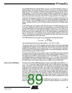
In fast PWM mode, the compare units allow generation of PWM waveforms on the
OC1x pins. Setting the COM1x1:0 bits to 2 will produce a non-inverted PWM and an
inverted PWM output can be generated by setting the COM1x1:0 to 3. See Table 37 on
page 96. The actual OC1x value will only be visible on the port pin if the data direction
for the port pin is set as output (DDR_OC1x). The PWM waveform is generated by set-
ting (or clearing) the OC1x Register at the Compare Match between OCR1x and
TCNT1, and clearing (or setting) the OC1x Register at the timer clock cycle the counter
is cleared (changes from TOP to BOTTOM).
The PWM frequency for the output can be calculated by the following equation:
f
clk_I/O
f
= ----------------------------------
OCnxPWM
N (1 + TOP)
The N variable represents the prescaler divider (1, 8, 64, 256, or 1024).
The extreme values for the OCR1x Register represents special cases when generating
a PWM waveform output in the fast PWM mode. If the OCR1x is set equal to BOTTOM
(0x0000) the output will be a narrow spike for each TOP+1 timer clock cycle. Setting the
OCR1x equal to TOP will result in a constant high or low output (depending on the polar-
ity of the output set by the COM1x1:0 bits.)
A frequency (with 50% duty cycle) waveform output in fast PWM mode can be achieved
by setting OC1A to toggle its logical level on each Compare Match (COM1A1:0 = 1).
This applies only if OCR1A is used to define the TOP value (WGM13:0 = 15). The wave-
form generated will have a maximum frequency of fOC A = fclk_I/O/2 when OCR1A is set to
1
zero (0x0000). This feature is similar to the OC1A toggle in CTC mode, except the dou-
ble buffer feature of the Output Compare unit is enabled in the fast PWM mode.
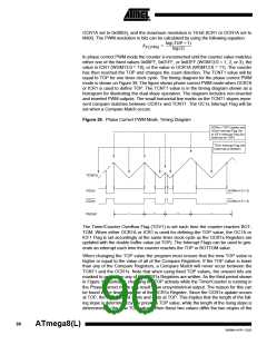
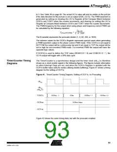
Phase Correct PWM Mode
The phase correct Pulse Width Modulation or phase correct PWM mode (WGM13:0 = 1,
2, 3, 10, or 11) provides a high resolution phase correct PWM waveform generation
option. The phase correct PWM mode is, like the phase and frequency correct PWM
mode, based on a dual-slope operation. The counter counts repeatedly from BOTTOM
(0x0000) to TOP and then from TOP to BOTTOM. In non-inverting Compare Output
mode, the Output Compare (OC1x) is cleared on the Compare Match between TCNT1
and OCR1x while upcounting, and set on the Compare Match while downcounting. In
inverting Output Compare mode, the operation is inverted. The dual-slope operation has
lower maximum operation frequency than single slope operation. However, due to the
symmetric feature of the dual-slope PWM modes, these modes are preferred for motor
control applications.
The PWM resolution for the phase correct PWM mode can be fixed to 8-, 9-, or 10-bit, or
defined by either ICR1 or OCR1A. The minimum resolution allowed is 2-bit (ICR1 or
89
2486M–AVR–12/03

 ATMEL [ ATMEL ]