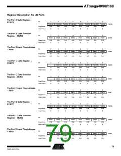
ATmega48/88/168
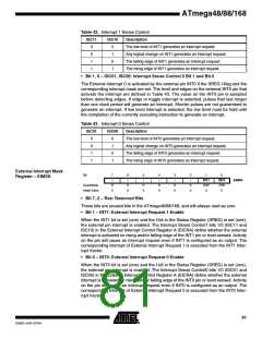
Pin Change Interrupt Flag
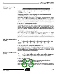
Register - PCIFR
Bit
7
–
6
–
5
–
4
–
3
–
2
PCIF2
R/W
0
1
PCIF1
R/W
0
0
PCIF0
R/W
0
PCIFR
Read/Write
Initial Value
R
0
R
0
R
0
R
0
R
0
• Bit 7..3 - Res: Reserved Bits
These bits are unused bits in the ATmega48/88/168, and will always read as zero.
• Bit 2 - PCIF2: Pin Change Interrupt Flag 2
When a logic change on any PCINT23..16 pin triggers an interrupt request, PCIF2
becomes set (one). If the I-bit in SREG and the PCIE2 bit in PCICR are set (one), the
MCU will jump to the corresponding Interrupt Vector. The flag is cleared when the inter-
rupt routine is executed. Alternatively, the flag can be cleared by writing a logical one to
it.
• Bit 1 - PCIF1: Pin Change Interrupt Flag 1
When a logic change on any PCINT14..8 pin triggers an interrupt request, PCIF1
becomes set (one). If the I-bit in SREG and the PCIE1 bit in PCICR are set (one), the
MCU will jump to the corresponding Interrupt Vector. The flag is cleared when the inter-
rupt routine is executed. Alternatively, the flag can be cleared by writing a logical one to
it.
• Bit 0 - PCIF0: Pin Change Interrupt Flag 0
When a logic change on any PCINT7..0 pin triggers an interrupt request, PCIF0
becomes set (one). If the I-bit in SREG and the PCIE0 bit in PCICR are set (one), the
MCU will jump to the corresponding Interrupt Vector. The flag is cleared when the inter-
rupt routine is executed. Alternatively, the flag can be cleared by writing a logical one to
it.
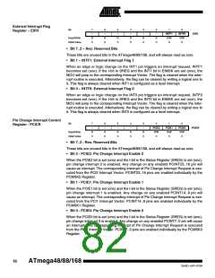
Pin Change Mask Register 2 –
PCMSK2
Bit
7
PCINT23
R/W
0
6
PCINT22
R/W
0
5
PCINT21
R/W
0
4
PCINT20
R/W
0
3
PCINT19
R/W
0
2
PCINT18
R/W
0
1
PCINT17
R/W
0
0
PCINT16
R/W
0
PCMSK2
Read/Write
Initial Value
• Bit 7..0 – PCINT23..16: Pin Change Enable Mask 23..16
Each PCINT23..16-bit selects whether pin change interrupt is enabled on the corre-
sponding I/O pin. If PCINT23..16 is set and the PCIE2 bit in PCICR is set, pin change
interrupt is enabled on the corresponding I/O pin. If PCINT23..16 is cleared, pin change
interrupt on the corresponding I/O pin is disabled.
Pin Change Mask Register 1 –
PCMSK1
Bit
7
–
6
PCINT14
R/W
0
5
PCINT13
R/W
0
4
PCINT12
R/W
0
3
PCINT11
R/W
0
2
PCINT10
R/W
0
1
PCINT9
R/W
0
0
PCINT8
R/W
0
PCMSK1
Read/Write
Initial Value
R
0
• Bit 7 – Res: Reserved Bit
This bit is an unused bit in the ATmega48/88/168, and will always read as zero.
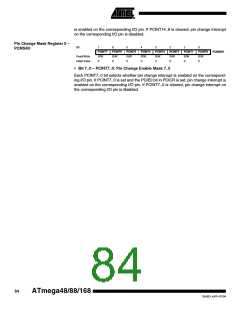
• Bit 6..0 – PCINT14..8: Pin Change Enable Mask 14..8
Each PCINT14..8-bit selects whether pin change interrupt is enabled on the correspond-
ing I/O pin. If PCINT14..8 is set and the PCIE1 bit in PCICR is set, pin change interrupt
83
2545D–AVR–07/04

 ATMEL [ ATMEL ]