ATmega48/88/168
Register Description for I/O Ports
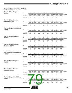
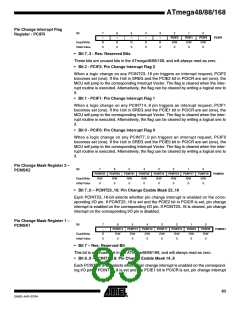
The Port B Data Register –
PORTB
Bit
7
PORTB7
R/W
0
6
PORTB6
R/W
0
5
PORTB5
R/W
0
4
PORTB4
R/W
0
3
PORTB3
R/W
0
2
PORTB2
R/W
0
1
PORTB1
R/W
0
0
PORTB0
R/W
0
PORTB
DDRB
PINB
Read/Write
Initial Value
The Port B Data Direction
Register – DDRB
Bit
7
DDB7
R/W
0
6
DDB6
R/W
0
5
DDB5
R/W
0
4
DDB4
R/W
0
3
DDB3
R/W
0
2
DDB2
R/W
0
1
DDB1
R/W
0
0
DDB0
R/W
0
Read/Write
Initial Value
The Port B Input Pins Address
– PINB
Bit
7
PINB7
R
6
PINB6
R
5
PINB5
R
4
PINB4
R
3
PINB3
R
2
PINB2
R
1
PINB1
R
0
PINB0
R
Read/Write
Initial Value
N/A
N/A
N/A
N/A
N/A
N/A
N/A
N/A
The Port C Data Register –
PORTC
Bit
7
–
6
PORTC6
R/W
0
5
PORTC5
R/W
0
4
PORTC4
R/W
0
3
PORTC3
R/W
0
2
PORTC2
R/W
0
1
PORTC1
R/W
0
0
PORTC0
R/W
0
PORTC
DDRC
PINC
Read/Write
Initial Value
R
0
The Port C Data Direction
Register – DDRC
Bit
7
–
6
DDC6
R/W
0
5
DDC5
R/W
0
4
DDC4
R/W
0
3
DDC3
R/W
0
2
DDC2
R/W
0
1
DDC1
R/W
0
0
DDC0
R/W
0
Read/Write
Initial Value
R
0
The Port C Input Pins Address
– PINC
Bit
7
–
6
PINC6
R
5
PINC5
R
4
PINC4
R
3
PINC3
R
2
PINC2
R
1
PINC1
R
0
PINC0
R
Read/Write
Initial Value
R
0
N/A
N/A
N/A
N/A
N/A
N/A
N/A
The Port D Data Register –
PORTD
Bit
7
PORTD7
R/W
0
6
PORTD6
R/W
0
5
PORTD5
R/W
0
4
PORTD4
R/W
0
3
PORTD3
R/W
0
2
PORTD2
R/W
0
1
PORTD1
R/W
0
0
PORTD0
R/W
0
PORTD
DDRD
PIND
Read/Write
Initial Value
The Port D Data Direction
Register – DDRD
Bit
7
DDD7
R/W
0
6
DDD6
R/W
0
5
DDD5
R/W
0
4
DDD4
R/W
0
3
DDD3
R/W
0
2
DDD2
R/W
0
1
DDD1
R/W
0
0
DDD0
R/W
0
Read/Write
Initial Value
The Port D Input Pins Address
– PIND
Bit
7
PIND7
R
6
PIND6
R
5
PIND5
R
4
PIND4
R
3
PIND3
R
2
PIND2
R
1
PIND1
R
0
PIND0
R
Read/Write
Initial Value
N/A
N/A
N/A
N/A
N/A
N/A
N/A
N/A
79
2545D–AVR–07/04

 ATMEL [ ATMEL ]