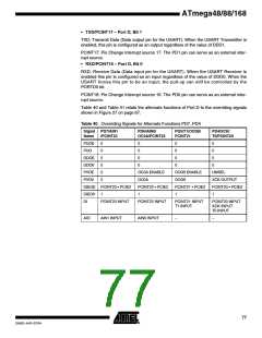
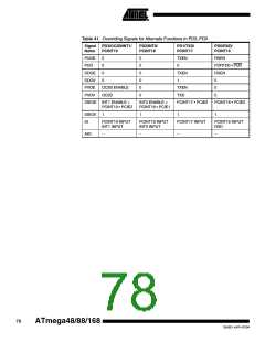
External Interrupts
The External Interrupts are triggered by the INT0 and INT1 pins or any of the
PCINT23..0 pins. Observe that, if enabled, the interrupts will trigger even if the INT0 and
INT1 or PCINT23..0 pins are configured as outputs. This feature provides a way of gen-
erating a software interrupt. The pin change interrupt PCI2 will trigger if any enabled
PCINT23..16 pin toggles. The pin change interrupt PCI1 will trigger if any enabled
PCINT14..8 pin toggles. The pin change interrupt PCI0 will trigger if any enabled
PCINT7..0 pin toggles. The PCMSK2, PCMSK1 and PCMSK0 Registers control which
pins contribute to the pin change interrupts. Pin change interrupts on PCINT23..0 are
detected asynchronously. This implies that these interrupts can be used for waking the
part also from sleep modes other than Idle mode.
The INT0 and INT1 interrupts can be triggered by a falling or rising edge or a low level.
This is set up as indicated in the specification for the External Interrupt Control Register
A – EICRA. When the INT0 or INT1 interrupts are enabled and are configured as level
triggered, the interrupts will trigger as long as the pin is held low. Note that recognition of
falling or rising edge interrupts on INT0 or INT1 requires the presence of an I/O clock,
described in “Clock Systems and their Distribution” on page 24. Low level interrupt on
INT0 and INT1 is detected asynchronously. This implies that this interrupt can be used
for waking the part also from sleep modes other than Idle mode. The I/O clock is halted
in all sleep modes except Idle mode.
Note that if a level triggered interrupt is used for wake-up from Power-down, the
required level must be held long enough for the MCU to complete the wake-up to trigger
the level interrupt. If the level disappears before the end of the Start-up Time, the MCU
will still wake up, but no interrupt will be generated. The start-up time is defined by the
SUT and CKSEL Fuses as described in “System Clock and Clock Options” on page 24.
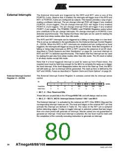
External Interrupt Control
Register A – EICRA
The External Interrupt Control Register A contains control bits for interrupt sense
control.
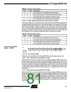
Bit
7
–
6
–
5
–
4
–
3
ISC11
R/W
0
2
ISC10
R/W
0
1
ISC01
R/W
0
0
ISC00
R/W
0
EICRA
Read/Write
Initial Value
R
0
R
0
R
0
R
0
• Bit 7..4 – Res: Reserved Bits
These bits are unused bits in the ATmega48/88/168, and will always read as zero.
• Bit 3, 2 – ISC11, ISC10: Interrupt Sense Control 1 Bit 1 and Bit 0
The External Interrupt 1 is activated by the external pin INT1 if the SREG I-flag and the
corresponding interrupt mask are set. The level and edges on the external INT1 pin that
activate the interrupt are defined in Table 42. The value on the INT1 pin is sampled
before detecting edges. If edge or toggle interrupt is selected, pulses that last longer
than one clock period will generate an interrupt. Shorter pulses are not guaranteed to
generate an interrupt. If low level interrupt is selected, the low level must be held until
the completion of the currently executing instruction to generate an interrupt.
80
ATmega48/88/168
2545D–AVR–07/04

 ATMEL [ ATMEL ]