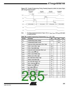
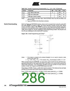
Table 129. Parallel Programming Characteristics, VCC = 5V 10ꢀ (Continued)
Symbol
tBVDV
Parameter
Min
Typ
Max
250
250
250
Units
ns
BS1 Valid to DATA valid
OE Low to DATA Valid
OE High to DATA Tri-stated
0
tOLDV
ns
tOHDZ
ns
Notes: 1. tWLRH is valid for the Write Flash, Write EEPROM, Write Fuse bits and Write Lock
bits commands.
2. tWLRH_CE is valid for the Chip Erase command.
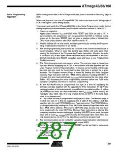
Serial Downloading
Both the Flash and EEPROM memory arrays can be programmed using the serial SPI
bus while RESET is pulled to GND. The serial interface consists of pins SCK, MOSI
(input) and MISO (output). After RESET is set low, the Programming Enable instruction
needs to be executed first before program/erase operations can be executed. NOTE, in
Table 128 on page 277, the pin mapping for SPI programming is listed. Not all parts use
the SPI pins dedicated for the internal SPI interface.
Figure 128. Serial Programming and Verify(1)
+1.8 - 5.5V
VCC
+1.8 - 5.5V(2)
MOSI
AVCC
MISO
SCK
XTAL1
RESET
GND
Notes: 1. If the device is clocked by the internal Oscillator, it is no need to connect a clock
source to the XTAL1 pin.
2. VCC - 0.3V < AVCC < VCC + 0.3V, however, AVCC should always be within 1.8 - 5.5V
When programming the EEPROM, an auto-erase cycle is built into the self-timed pro-
gramming operation (in the Serial mode ONLY) and there is no need to first execute the
Chip Erase instruction. The Chip Erase operation turns the content of every memory
location in both the Program and EEPROM arrays into 0xFF.
Depending on CKSEL Fuses, a valid clock must be present. The minimum low and high
periods for the serial clock (SCK) input are defined as follows:
Low:> 2 CPU clock cycles for fck < 12 MHz, 3 CPU clock cycles for fck >= 12 MHz
High:> 2 CPU clock cycles for fck < 12 MHz, 3 CPU clock cycles for fck >= 12 MHz
286
ATmega48/88/168
2545D–AVR–07/04

 ATMEL [ ATMEL ]