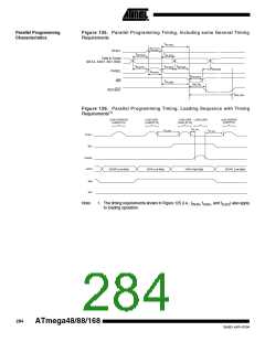
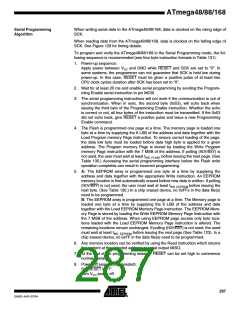
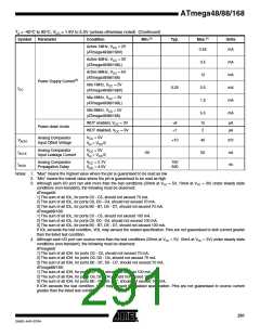
ATmega48/88/168
Serial Programming
Algorithm
When writing serial data to the ATmega48/88/168, data is clocked on the rising edge of
SCK.
When reading data from the ATmega48/88/168, data is clocked on the falling edge of
SCK. See Figure 129 for timing details.
To program and verify the ATmega48/88/168 in the Serial Programming mode, the fol-
lowing sequence is recommended (see four byte instruction formats in Table 131):
1. Power-up sequence:
Apply power between VCC and GND while RESET and SCK are set to “0”. In
some systems, the programmer can not guarantee that SCK is held low during
power-up. In this case, RESET must be given a positive pulse of at least two
CPU clock cycles duration after SCK has been set to “0”.
2. Wait for at least 20 ms and enable serial programming by sending the Program-
ming Enable serial instruction to pin MOSI.
3. The serial programming instructions will not work if the communication is out of
synchronization. When in sync. the second byte (0x53), will echo back when
issuing the third byte of the Programming Enable instruction. Whether the echo
is correct or not, all four bytes of the instruction must be transmitted. If the 0x53
did not echo back, give RESET a positive pulse and issue a new Programming
Enable command.
4. The Flash is programmed one page at a time. The memory page is loaded one
byte at a time by supplying the 6 LSB of the address and data together with the
Load Program memory Page instruction. To ensure correct loading of the page,
the data low byte must be loaded before data high byte is applied for a given
address. The Program memory Page is stored by loading the Write Program
memory Page instruction with the 7 MSB of the address. If polling (RDY/BSY) is
not used, the user must wait at least tWD_FLASH before issuing the next page. (See
Table 130.) Accessing the serial programming interface before the Flash write
operation completes can result in incorrect programming.
5. A: The EEPROM array is programmed one byte at a time by supplying the
address and data together with the appropriate Write instruction. An EEPROM
memory location is first automatically erased before new data is written. If polling
(RDY/BSY) is not used, the user must wait at least tWD_EEPROM before issuing the
next byte. (See Table 130.) In a chip erased device, no 0xFFs in the data file(s)
need to be programmed.
B: The EEPROM array is programmed one page at a time. The Memory page is
loaded one byte at a time by supplying the 6 LSB of the address and data
together with the Load EEPROM Memory Page instruction. The EEPROM Mem-
ory Page is stored by loading the Write EEPROM Memory Page Instruction with
the 7 MSB of the address. When using EEPROM page access only byte loca-
tions loaded with the Load EEPROM Memory Page instruction is altered. The
remaining locations remain unchanged. If polling (RDY/BSY) is not used, the used
must wait at least tWD_EEPROM before issuing the next page (See Table 123). In a
chip erased device, no 0xFF in the data file(s) need to be programmed.
6. Any memory location can be verified by using the Read instruction which returns
the content at the selected address at serial output MISO.
7. At the end of the programming session, RESET can be set high to commence
normal operation.
8. Power-off sequence (if needed):
Set RESET to “1”.
Turn VCC power off.
287
2545D–AVR–07/04

 ATMEL [ ATMEL ]