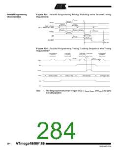
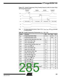
.
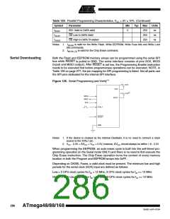
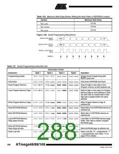
Table 130. Minimum Wait Delay Before Writing the Next Flash or EEPROM Location
Symbol
Minimum Wait Delay
4.5 ms
tWD_FLASH
tWD_EEPROM
tWD_ERASE
3.6 ms
9.0 ms
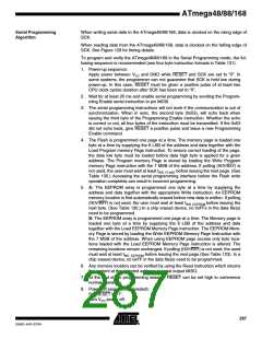
Figure 129. Serial Programming Waveforms
SERIAL DATA INPUT
(MOSI)
MSB
LSB
LSB
SERIAL DATA OUTPUT
(MISO)
MSB
SERIAL CLOCK INPUT
(SCK)
SAMPLE
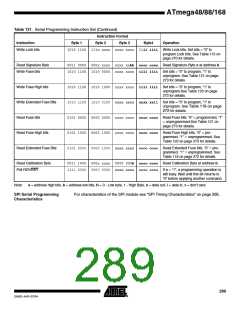
Table 131. Serial Programming Instruction Set
Instruction Format
Byte 2 Byte 3
Instruction
Byte 1
Byte4
Operation
Programming Enable
1010 1100 0101 0011 xxxx xxxx xxxx xxxx Enable Serial Programming after
RESET goes low.
Chip Erase
1010 1100 100x xxxx xxxx xxxx xxxx xxxx Chip Erase EEPROM and Flash.
Read Program Memory
0010 H000 000a aaaa bbbb bbbb oooo oooo Read H (high or low) data o from
Program memory at word address a:b.
Load Program Memory Page
0100 H000 000x xxxx xxxx bbbb iiii iiii Write H (high or low) data i to Program
Memory page at word address b. Data
low byte must be loaded before Data
high byte is applied within the same
address.
Write Program Memory Page 0100 1100 000a aaaa bbbb xxxx xxxx xxxx Write Program Memory Page at
address a:b.
Read EEPROM Memory
1010 0000 000x xxaa bbbb bbbb oooo oooo Read data o from EEPROM memory at
address a:b.
Write EEPROM Memory
1100 0000 000x xxaa bbbb bbbb iiii iiii Write data i to EEPROM memory at
address a:b.
Load EEPROM Memory
Page (page access)
1100 0001 0000 0000 0000 00bb iiii iiii Load data i to EEPROM memory page
buffer. After data is loaded, program
EEPROM page.
Write EEPROM Memory
Page (page access)
1100 0010 00xx xxaa bbbb bb00 xxxx xxxx
Write EEPROM page at address a:b.
Read Lock bits
0101 1000 0000 0000 xxxx xxxx xxoo oooo Read Lock bits. “0” = programmed, “1”
= unprogrammed. See Table 115 on
page 270 for details.
288
ATmega48/88/168
2545D–AVR–07/04

 ATMEL [ ATMEL ]