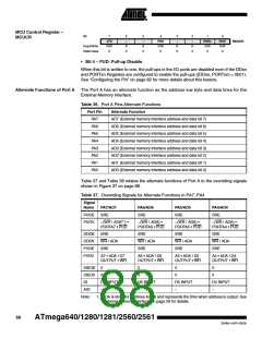
MCU Control Register –
MCUCR
Bit
7
6
–
5
–
4
3
–
2
–
1
IVSEL
R/W
0
0
IVCE
R/W
0
JTD
R/W
0
PUD
R/W
0
MCUCR
Read/Write
Initial Value
R
0
R
0
R
0
R
0
• Bit 4 – PUD: Pull-up Disable
When this bit is written to one, the pull-ups in the I/O ports are disabled even if the DDxn
and PORTxn Registers are configured to enable the pull-ups ({DDxn, PORTxn} = 0b01).
See “Configuring the Pin” on page 82 for more details about this feature.
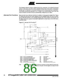
Alternate Functions of Port A The Port A has an alternate function as the address low byte and data lines for the
External Memory Interface.
Table 36. Port A Pins Alternate Functions
Port Pin
PA7
Alternate Function
AD7 (External memory interface address and data bit 7)
AD6 (External memory interface address and data bit 6)
AD5 (External memory interface address and data bit 5)
AD4 (External memory interface address and data bit 4)
AD3 (External memory interface address and data bit 3)
AD2 (External memory interface address and data bit 2)
AD1 (External memory interface address and data bit 1)
AD0 (External memory interface address and data bit 0)
PA6
PA5
PA4
PA3
PA2
PA1
PA0
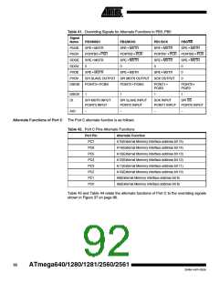
Table 37 and Table 38 relates the alternate functions of Port A to the overriding signals
shown in Figure 37 on page 86.
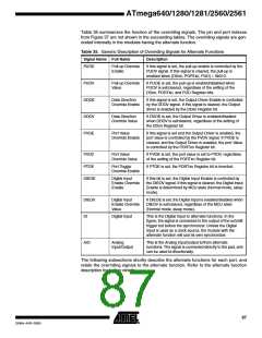
Table 37. Overriding Signals for Alternate Functions in PA7..PA4
Signal
Name
PUOE
PUOV
PA7/AD7
PA6/AD6
PA5/AD5
PA4/AD4
SRE
SRE
SRE
SRE
~(WR | ADA(1)) •
PORTA7 • PUD
~(WR | ADA) •
PORTA6 • PUD
~(WR | ADA) •
PORTA5 • PUD
~(WR | ADA) •
PORTA4 • PUD
DDOE
DDOV
PVOE
PVOV
SRE
SRE
SRE
SRE
WR | ADA
SRE
WR | ADA
SRE
WR | ADA
SRE
WR | ADA
SRE
A7 • ADA | D7
OUTPUT • WR
A6 • ADA | D6
OUTPUT • WR
A5 • ADA | D5
OUTPUT • WR
A4 • ADA | D4
OUTPUT • WR
DIEOE
DIEOV
DI
0
0
0
0
0
0
0
0
D7 INPUT
–
D6 INPUT
–
D5 INPUT
–
D4 INPUT
–
AIO
Note:
1. ADA is short for ADdress Active and represents the time when address is output. See
“External Memory Interface” on page 29 for details.
88
ATmega640/1280/1281/2560/2561
2549A–AVR–03/05

 ATMEL [ ATMEL ]