ATmega8U2/16U2/32U2
For a detailed description of SPI, debugWIRE and Parallel data downloading to the EEPROM,
see page 259, page 244, and page 250 respectively.
7.3.1
EEPROM Read/Write Access
The EEPROM Access Registers are accessible in the I/O space.
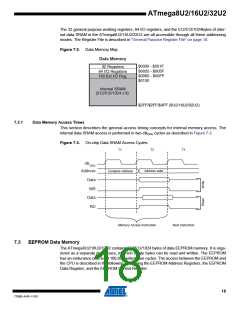
The write access time for the EEPROM is given in Table 7-2 on page 22. A self-timing function,
however, lets the user software detect when the next byte can be written. If the user code con-
tains instructions that write the EEPROM, some precautions must be taken. In heavily filtered
power supplies, VCC is likely to rise or fall slowly on power-up/down. This causes the device for
some period of time to run at a voltage lower than specified as minimum for the clock frequency
used. See “Preventing EEPROM Corruption” on page 19. for details on how to avoid problems in
these situations.
In order to prevent unintentional EEPROM writes, a specific write procedure must be followed.
Refer to the description of the EEPROM Control Register for details on this.
When the EEPROM is read, the CPU is halted for four clock cycles before the next instruction is
executed. When the EEPROM is written, the CPU is halted for two clock cycles before the next
instruction is executed.
7.3.2
Preventing EEPROM Corruption
During periods of low VCC, the EEPROM data can be corrupted because the supply voltage is
too low for the CPU and the EEPROM to operate properly. These issues are the same as for
board level systems using EEPROM, and the same design solutions should be applied.
An EEPROM data corruption can be caused by two situations when the voltage is too low. First,
a regular write sequence to the EEPROM requires a minimum voltage to operate correctly. Sec-
ondly, the CPU itself can execute instructions incorrectly, if the supply voltage is too low.
EEPROM data corruption can easily be avoided by following this design recommendation:
Keep the AVR RESET active (low) during periods of insufficient power supply voltage. This can
be done by enabling the internal Brown-out Detector (BOD). If the detection level of the internal
BOD does not match the needed detection level, an external low VCC reset Protection circuit can
be used. If a reset occurs while a write operation is in progress, the write operation will be com-
pleted provided that the power supply voltage is sufficient.
7.4
I/O Memory
The I/O space definition of the ATmega8U2/16U2/32U2 is shown in “Register Summary” on
page 288.
All ATmega8U2/16U2/32U2 I/Os and peripherals are placed in the I/O space. All I/O locations
may be accessed by the LD/LDS/LDD and ST/STS/STD instructions, transferring data between
the 32 general purpose working registers and the I/O space. I/O Registers within the address
range 0x00 - 0x1F are directly bit-accessible using the SBI and CBI instructions. In these regis-
ters, the value of single bits can be checked by using the SBIS and SBIC instructions. Refer to
the instruction set section for more details. When using the I/O specific commands IN and OUT,
the I/O addresses 0x00 - 0x3F must be used. When addressing I/O Registers as data space
using LD and ST instructions, 0x20 must be added to these addresses. The
ATmega8U2/16U2/32U2 is a complex microcontroller with more peripheral units than can be
supported within the 64 location reserved in Opcode for the IN and OUT instructions. For the
19
7799D–AVR–11/10

 ATMEL [ ATMEL ]