ATmega8U2/16U2/32U2
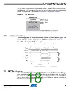
The 32 general purpose working registers, 64 I/O registers, and the 512/512/1024bytes of inter-
nal data SRAM in the ATmega8U2/16U2/32U2 are all accessible through all these addressing
modes. The Register File is described in “General Purpose Register File” on page 10.
Figure 7-2. Data Memory Map
Data Memory
$0000 - $001F
$0020 - $005F
$0060 - $00FF
$0100
32 Registers
64 I/O Registers
160 Ext I/O Reg.
Internal SRAM
(512/512/1024 x 8)
$2FF/$2FF/$4FF (8U2/16U2/32U2)
7.2.1
Data Memory Access Times
This section describes the general access timing concepts for internal memory access. The
internal data SRAM access is performed in two clkCPU cycles as described in Figure 7-3.
Figure 7-3. On-chip Data SRAM Access Cycles
T1
T2
T3
clkCPU
Address valid
Compute Address
Address
Data
WR
Data
RD
Memory Access Instruction
Next Instruction
7.3
EEPROM Data Memory
The ATmega8U2/16U2/32U2 contains 512/512/1024 bytes of data EEPROM memory. It is orga-
nized as a separate data space, in which single bytes can be read and written. The EEPROM
has an endurance of at least 100,000 write/erase cycles. The access between the EEPROM and
the CPU is described in the following, specifying the EEPROM Address Registers, the EEPROM
Data Register, and the EEPROM Control Register.
18
7799D–AVR–11/10

 ATMEL [ ATMEL ]