ATmega640/1280/1281/2560/2561
• Bit 7 – FOCnA: Force Output Compare for Channel A
• Bit 6 – FOCnB: Force Output Compare for Channel B
• Bit 5 – FOCnC: Force Output Compare for Channel C
The FOCnA/FOCnB/FOCnC bits are only active when the WGMn3:0 bits specifies a non-PWM
mode. When writing a logical one to the FOCnA/FOCnB/FOCnC bit, an immediate compare
match is forced on the waveform generation unit. The OCnA/OCnB/OCnC output is changed
according to its COMnx1:0 bits setting. Note that the FOCnA/FOCnB/FOCnC bits are imple-
mented as strobes. Therefore it is the value present in the COMnx1:0 bits that determine the
effect of the forced compare.
A FOCnA/FOCnB/FOCnC strobe will not generate any interrupt nor will it clear the timer in Clear
Timer on Compare Match (CTC) mode using OCRnA as TOP.
The FOCnA/FOCnB/FOCnB bits are always read as zero.
• Bit 4:0 – Reserved Bits
These bits are reserved for future use. For ensuring compatibility with future devices, these bits
must be written to zero when TCCRnC is written.
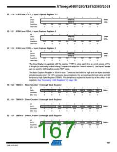
17.11.13 TCNT1H and TCNT1L – Timer/Counter 1
Bit
7
6
5
4
3
2
1
0
(0x85)
TCNT1[15:8]
TCNT1[7:0]
TCNT1H
TCNT1L
(0x84)
Read/Write
Initial Value
R/W
R/W
R/W
R/W
R/W
R/W
R/W
R/W
0
0
0
0
0
0
0
0
17.11.14 TCNT3H and TCNT3L – Timer/Counter 3
Bit
7
6
5
4
3
2
1
0
(0x95)
TCNT3[15:8]
TCNT3[7:0]
TCNT3H
TCNT3L
(0x94)
Read/Write
Initial Value
R/W
R/W
R/W
R/W
R/W
R/W
R/W
R/W
0
0
0
0
0
0
0
0
17.11.15 TCNT4H and TCNT4L –Timer/Counter 4
Bit
7
6
5
4
3
2
1
0
(0xA5)
TCNT4[15:8]
TCNT4[7:0]
TCNT4H
TCNT4L
(0xA4)
Read/Write
Initial Value
R/W
R/W
R/W
R/W
R/W
R/W
R/W
R/W
0
0
0
0
0
0
0
0
17.11.16 TCNT5H and TCNT5L –Timer/Counter 5
Bit
7
6
5
4
3
2
1
0
(0x125)
(0x124)
Read/Write
Initial Value
TCNT5[15:8]
TCNT5[7:0]
TCNT5H
TCNT5L
R/W
R/W
R/W
R/W
R/W
R/W
R/W
R/W
0
0
0
0
0
0
0
0
The two Timer/Counter I/O locations (TCNTnH and TCNTnL, combined TCNTn) give direct
access, both for read and for write operations, to the Timer/Counter unit 16-bit counter. To
ensure that both the high and low bytes are read and written simultaneously when the CPU
accesses these registers, the access is performed using an 8-bit temporary High Byte Register
163
2549L–AVR–08/07

 ATMEL [ ATMEL ]