ATmega640/1280/1281/2560/2561
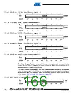
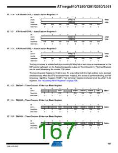
17.11.30 ICR3H and ICR3L – Input Capture Register 3 –
Bit
7
6
5
4
3
2
1
0
(0x97)
ICR3[15:8]
ICR3[7:0]
ICR3H
ICR3L
(0x96)
Read/Write
Initial Value
R/W
R/W
R/W
R/W
R/W
R/W
R/W
R/W
0
0
0
0
0
0
0
0
17.11.31 ICR4H and ICR4L – Input Capture Register 4
Bit
7
6
5
4
3
2
1
0
(0xA7)
ICR4[15:8]
ICR4[7:0]
ICR4H
ICR4L
(0xA6)
Read/Write
Initial Value
R/W
R/W
R/W
R/W
R/W
R/W
R/W
R/W
0
0
0
0
0
0
0
0
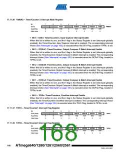
17.11.32 ICR5H and ICR5L – Input Capture Register 5
Bit
7
6
5
4
3
2
1
0
(0x127)
(0x126)
Read/Write
Initial Value
ICR5[15:8]
ICR5[7:0]
ICR5H
ICR5L
R/W
R/W
R/W
R/W
R/W
R/W
R/W
R/W
0
0
0
0
0
0
0
0
The Input Capture is updated with the counter (TCNTn) value each time an event occurs on the
ICPn pin (or optionally on the Analog Comparator output for Timer/Counter1). The Input Capture
can be used for defining the counter TOP value.
The Input Capture Register is 16-bit in size. To ensure that both the high and low bytes are read
simultaneously when the CPU accesses these registers, the access is performed using an 8-bit
temporary High Byte Register (TEMP). This temporary register is shared by all the other 16-bit
registers. See “Accessing 16-bit Registers” on page 138.
17.11.33 TIMSK1 – Timer/Counter 1 Interrupt Mask Register
Bit
(0x6F)
7
6
5
4
–
3
OCIE1C
R/W
0
2
OCIE1B
R/W
0
1
OCIE1A
R/W
0
0
TOIE1
R/W
0
–
–
ICIE1
TIMSK1
TIMSK3
TIMSK4
Read/Write
R
0
R
0
R/W
R
0
Initial Value
0
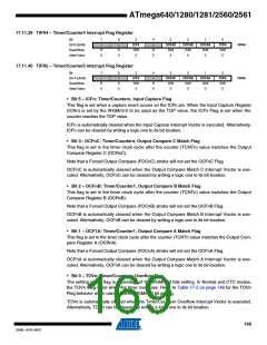
17.11.34 TIMSK3 – Timer/Counter 3 Interrupt Mask Register
Bit
7
–
6
–
5
ICIE3
R/W
0
4
–
3
OCIE3C
R/W
0
2
OCIE3B
R/W
0
1
OCIE3A
R/W
0
0
TOIE3
R/W
0
(0x71)
Read/Write
Initial Value
R
0
R
0
R
0
17.11.35 TIMSK4 – Timer/Counter 4 Interrupt Mask Register
Bit
7
–
6
–
5
ICIE4
R/W
0
4
–
3
OCIE4C
R/W
0
2
OCIE4B
R/W
0
1
OCIE4A
R/W
0
0
TOIE4
R/W
0
(0x72)
Read/Write
Initial Value
R
0
R
0
R
0
167
2549L–AVR–08/07

 ATMEL [ ATMEL ]