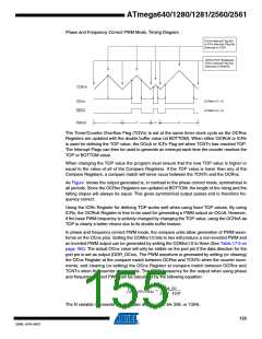
ATmega640/1280/1281/2560/2561
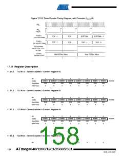
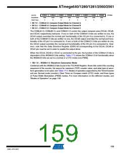
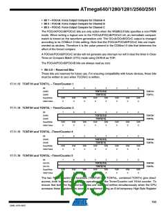
COM5A1
R/W
0
COM5A0
R/W
0
COM5B1
R/W
0
COM5B0
R/W
0
COM5C1
R/W
0
COM5C0
R/W
0
WGM51
R/W
0
WGM50
R/W
0
TCCR5A
(0x120)
Read/Write
Initial Value
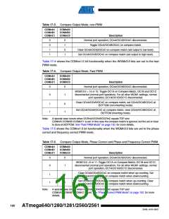
• Bit 7:6 – COMnA1:0: Compare Output Mode for Channel A
• Bit 5:4 – COMnB1:0: Compare Output Mode for Channel B
• Bit 3:2 – COMnC1:0: Compare Output Mode for Channel C
The COMnA1:0, COMnB1:0, and COMnC1:0 control the output compare pins (OCnA, OCnB,
and OCnC respectively) behavior. If one or both of the COMnA1:0 bits are written to one, the
OCnA output overrides the normal port functionality of the I/O pin it is connected to. If one or
both of the COMnB1:0 bits are written to one, the OCnB output overrides the normal port func-
tionality of the I/O pin it is connected to. If one or both of the COMnC1:0 bits are written to one,
the OCnC output overrides the normal port functionality of the I/O pin it is connected to. How-
ever, note that the Data Direction Register (DDR) bit corresponding to the OCnA, OCnB or
OCnC pin must be set in order to enable the output driver.
When the OCnA, OCnB or OCnC is connected to the pin, the function of the COMnx1:0 bits is
dependent of the WGMn3:0 bits setting. Table 17-3 shows the COMnx1:0 bit functionality when
the WGMn3:0 bits are set to a normal or a CTC mode (non-PWM).
• Bit 1:0 – WGMn1:0: Waveform Generation Mode
Combined with the WGMn3:2 bits found in the TCCRnB Register, these bits control the counting
sequence of the counter, the source for maximum (TOP) counter value, and what type of wave-
form generation to be used, see Table 17-2. Modes of operation supported by the Timer/Counter
unit are: Normal mode (counter), Clear Timer on Compare match (CTC) mode, and three types
of Pulse Width Modulation (PWM) modes. For more information on the different modes, see
“Modes of Operation” on page 148.
159
2549L–AVR–08/07

 ATMEL [ ATMEL ]