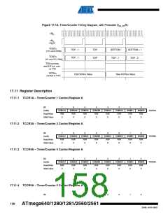
• Bit 2:0 – CSn2:0: Clock Select
The three clock select bits select the clock source to be used by the Timer/Counter, see Figure
17-9 and Figure 17-10.
Table 17-6. Clock Select Bit Description
CSn2
CSn1
CSn0
Description
No clock source. (Timer/Counter stopped)
clkI/O/1 (No prescaling
0
0
0
0
1
1
1
1
0
0
1
1
0
0
1
1
0
1
0
1
0
1
0
1
clkI/O/8 (From prescaler)
clkI/O/64 (From prescaler)
clkI/O/256 (From prescaler)
clkI/O/1024 (From prescaler)
External clock source on Tn pin. Clock on falling edge
External clock source on Tn pin. Clock on rising edge
If external pin modes are used for the Timer/Countern, transitions on the Tn pin will clock the
counter even if the pin is configured as an output. This feature allows software control of the
counting.
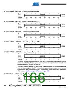
17.11.9 TCCR1C – Timer/Counter 1 Control Register C
Bit
(0x82)
7
6
5
4
–
3
–
2
–
1
–
0
–
FOC1A
FOC1B
FOC1C
TCCR1C
TCCR3C
TCCR4C
TCCR5C
Read/Write
W
W
W
R
0
R
0
R
0
R
0
R
0
Initial Value
0
0
0
17.11.10 TCCR3C – Timer/Counter 3 Control Register C
Bit
7
FOC3A
W
6
FOC3B
W
5
FOC3C
W
4
–
3
–
2
–
1
–
0
–
(0x92)
Read/Write
Initial Value
R
0
R
0
R
0
R
0
R
0
0
0
0
17.11.11 TCCR4C – Timer/Counter 4 Control Register C
Bit
7
FOC4A
W
6
FOC4B
W
5
FOC4C
W
4
–
3
–
2
–
1
–
0
–
(0xA2)
Read/Write
Initial Value
R
0
R
0
R
0
R
0
R
0
0
0
0
17.11.12 TCCR5C – Timer/Counter 5 Control Register C
Bit
7
FOC5A
W
6
FOC5B
W
5
FOC3C
W
4
–
3
–
2
–
1
–
0
–
(0x122)
Read/Write
Initial Value
R
0
R
0
R
0
R
0
R
0
0
0
0
162
ATmega640/1280/1281/2560/2561
2549L–AVR–08/07

 ATMEL [ ATMEL ]