• Bit 7 – AMP0EN: Amplifier 0 Enable Bit
Set this bit to enable the Amplifier 0.
Clear this bit to disable the Amplifier 0.
Clearing this bit while a conversion is running will take effect at the end of the conversion.
Warning: Always clear AMP0TS1:0 when clearing AMP0EN.
• Bit 6– AMP0IS: Amplifier 0 Input Shunt
Set this bit to short-circuit the Amplifier 0 input.
Clear this bit to normally use the Amplifier 0.
• Bit 5, 4– AMP0G1, 0: Amplifier 0 Gain Selection Bits
These 2 bits determine the gain of the amplifier 0.
The different setting are shown in Table 21-8.
Table 21-8. Amplifier 0 Gain Selection
AMP0G1
AMP0G0
Description
Gain 5
0
0
1
1
0
1
0
1
Gain 10
Gain 20
Gain 40
To ensure an accurate result, after the gain value has been changed, the amplifier input needs
to have a quite stable input value during at least 4 Amplifier synchronization clock periods.
• Bit 1, 0– AMP0TS1, AMP0TS0: Amplifier 0 Trigger Source Selection Bits
In accordance with the Table 21-9, these 2 bits select the event which will generate the trigger
for the amplifier 0. This trigger source is necessary to start the conversion on the amplified
channel.
Table 21-9. AMP0 Auto Trigger Source Selection
AMP0TS1
AMP0TS0
Description
0
0
1
1
0
1
0
1
Auto synchronization on ADC Clock/8
Trig on PSC0ASY
Trig on PSC1ASY
Trig on PSC2ASY
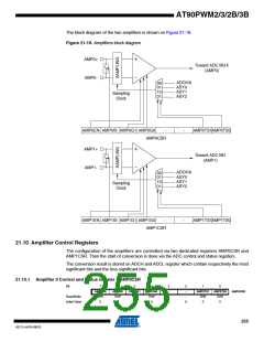
21.10.2 Amplifier 1Control and Status register – AMP1CSR
Bit
7
AMP1EN
R/W
6
AMP1IS
R/W
0
5
AMP1G1
R/W
0
4
AMP1G0
R/W
0
3
-
2
-
1
AMP1TS1
R/W
0
AMP1TS0
R/W
AMP1CSR
Read/Write
Initial Value
-
-
0
0
0
0
0
• Bit 7 – AMP1EN: Amplifier 1 Enable Bit
Set this bit to enable the Amplifier 1.
Clear this bit to disable the Amplifier 1.
Clearing this bit while a conversion is running will take effect at the end of the conversion.
Warning: Always clear AMP1TS1:0 when clearing AMP1EN.
• Bit 6– AMP1IS: Amplifier 1 Input Shunt
256
AT90PWM2/3/2B/3B
4317J–AVR–08/10

 ATMEL [ ATMEL ]