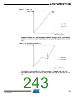
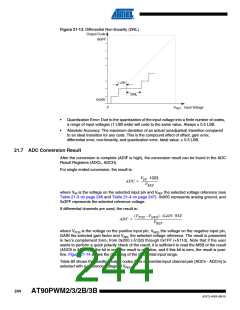
Figure 21-13. Differential Non-linearity (DNL)
Output Code
0x3FF
1 LSB
DNL
0x000
0
V
Input Voltage
REF
•
•
Quantization Error: Due to the quantization of the input voltage into a finite number of codes,
a range of input voltages (1 LSB wide) will code to the same value. Always 0.5 LSB.
Absolute Accuracy: The maximum deviation of an actual (unadjusted) transition compared
to an ideal transition for any code. This is the compound effect of offset, gain error,
differential error, non-linearity, and quantization error. Ideal value: 0.5 LSB.
21.7 ADC Conversion Result
After the conversion is complete (ADIF is high), the conversion result can be found in the ADC
Result Registers (ADCL, ADCH).
For single ended conversion, the result is:
V
⋅ 1023
IN
ADC = --------------------------
V
REF
where VIN is the voltage on the selected input pin and VREF the selected voltage reference (see
Table 21-3 on page 246 and Table 21-4 on page 247). 0x000 represents analog ground, and
0x3FF represents the selected reference voltage.
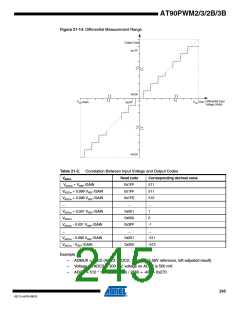
If differential channels are used, the result is:
(V
– V
) ⋅ GAIN ⋅ 512
NEG
POS
ADC = ------------------------------------------------------------------------
V
REF
where VPOS is the voltage on the positive input pin, VNEG the voltage on the negative input pin,
GAIN the selected gain factor and VREF the selected voltage reference. The result is presented
in two’s complement form, from 0x200 (-512d) through 0x1FF (+511d). Note that if the user
wants to perform a quick polarity check of the result, it is sufficient to read the MSB of the result
(ADC9 in ADCH). If the bit is one, the result is negative, and if this bit is zero, the result is posi-
tive. Figure 21-14 shows the decoding of the differential input range.
Table 82 shows the resulting output codes if the differential input channel pair (ADCn - ADCm) is
selected with a reference voltage of VREF
.
244
AT90PWM2/3/2B/3B
4317J–AVR–08/10

 ATMEL [ ATMEL ]