–
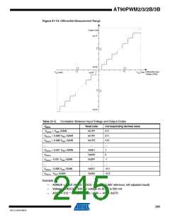
ADCL will thus read 0x00, and ADCH will read 0x9C.
Writing zero to ADLAR right adjusts the result: ADCL = 0x70, ADCH = 0x02.
Example 2:
–
–
–
–
ADMUX = 0xFB (ADC3 - ADC2, 1x gain, 2.56V reference, left adjusted result)
Voltage on ADC3 is 300 mV, voltage on ADC2 is 500 mV.
ADCR = 512 * 1 * (300 - 500) / 2560 = -41 = 0x029.
ADCL will thus read 0x40, and ADCH will read 0x0A.
Writing zero to ADLAR right adjusts the result: ADCL = 0x00, ADCH = 0x29.
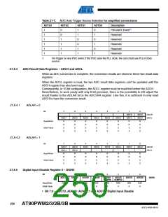
21.8 ADC Register Description
The ADC of the AT90PWM2/2B/3/3B is controlled through 3 different registers. The ADCSRA
and The ADCSRB registers which are the ADC Control and Status registers, and the ADMUX
which allows to select the Vref source and the channel to be converted.
The conversion result is stored on ADCH and ADCL register which contain respectively the most
significant bits and the less significant bits.
21.8.1
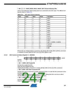
ADC Multiplexer Register – ADMUX
Bit
7
6
REFS0
R/W
0
5
ADLAR
R/W
0
4
-
3
MUX3
R/W
0
2
MUX2
R/W
0
1
MUX1
R/W
0
0
MUX0
R/W
0
REFS1
R/W
0
ADMUX
Read/Write
Initial Value
-
0
• Bit 7, 6 – REFS1, 0: ADC Vref Selection Bits
These 2 bits determine the voltage reference for the ADC.
The different setting are shown in Table 21-3.
Table 21-3. ADC Voltage Reference Selection
REFS1
REFS0
Description
External Vref on AREF pin, Internal Vref is switched off
0
0
1
0
1
0
AVcc with external capacitor connected on the AREF pin
Reserved
Internal 2.56V Reference voltage with external capacitor connected on
the AREF pin
1
1
If these bits are changed during a conversion, the change will not take effect until this conversion
is complete (it means while the ADIF bit in ADCSRA register is set).
In case the internal Vref is selected, it is turned ON as soon as an analog feature needed it is
set.
• Bit 5 – ADLAR: ADC Left Adjust Result
Set this bit to left adjust the ADC result.
Clear it to right adjust the ADC result.
The ADLAR bit affects the configuration of the ADC result data registers. Changing this bit
affects the ADC data registers immediately regardless of any on going conversion. For a com-
plete description of this bit, see Section “ADC Result Data Registers – ADCH and ADCL”,
page 250.
246
AT90PWM2/3/2B/3B
4317J–AVR–08/10

 ATMEL [ ATMEL ]