AT90PWM2/3/2B/3B
OCR1B[7:0]
OCR1BL
Read/Write
Initial Value
R/W
0
R/W
0
R/W
0
R/W
R/W
0
R/W
0
R/W
0
R/W
0
0
The Output Compare Registers contain a 16-bit value that is continuously compared with the
counter value (TCNTn). A match can be used to generate an Output Compare interrupt, or to
generate a waveform output on the OCnx pin.
The Output Compare Registers are 16-bit in size. To ensure that both the high and low bytes are
written simultaneously when the CPU writes to these registers, the access is performed using an
8-bit temporary High Byte Register (TEMP). This temporary register is shared by all the other
16-bit registers. See “Accessing 16-bit Registers” on page 104.
15.10.7 Input Capture Register 1 – ICR1H and ICR1L
Bit
7
6
5
4
3
2
1
0
ICR1[15:8]
ICR1[7:0]
ICR1H
ICR1L
Read/Write
Initial Value
R/W
R/W
R/W
0
R/W
0
R/W
0
R/W
0
R/W
0
R/W
0
0
0
The Input Capture is updated with the counter (TCNTn) value each time an event occurs on the
ICPn pin (or optionally on the Analog Comparator output for Timer/Counter1). The Input Capture
can be used for defining the counter TOP value.
The Input Capture Register is 16-bit in size. To ensure that both the high and low bytes are read
simultaneously when the CPU accesses these registers, the access is performed using an 8-bit
temporary High Byte Register (TEMP). This temporary register is shared by all the other 16-bit
registers. See “Accessing 16-bit Registers” on page 104.
15.10.8 Timer/Counter1 Interrupt Mask Register – TIMSK1
Bit
7
6
5
4
–
3
–
2
OCIE1B
R/W
0
1
OCIE1A
R/W
0
0
TOIE1
R/W
0
–
–
ICIE1
TIMSK1
Read/Write
Initial Value
R
0
R
0
R/W
0
R
0
R
0
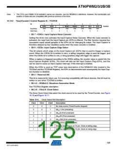
• Bit 7, 6 – Res: Reserved Bits
These bits are unused bits in the AT90PWM2/2B/3/3B, and will always read as zero.
• Bit 5 – ICIE1: Timer/Counter1, Input Capture Interrupt Enable
When this bit is written to one, and the I-flag in the Status Register is set (interrupts globally
enabled), the Timer/Counter1 Input Capture interrupt is enabled. The corresponding Interrupt
Vector (see “Reset and Interrupt Vectors Placement in AT90PWM2/2B/3/3B(1)” on page 57) is
executed when the ICF1 Flag, located in TIFR1, is set.
• Bit 4, 3 – Res: Reserved Bits
These bits are unused bits in the AT90PWM2/2B/3/3B, and will always read as zero.
• Bit 2 – OCIE1B: Timer/Counter1, Output Compare B Match Interrupt Enable
When this bit is written to one, and the I-flag in the Status Register is set (interrupts globally
enabled), the Timer/Counter1 Output Compare B Match interrupt is enabled. The corresponding
Interrupt Vector (see “Reset and Interrupt Vectors Placement in AT90PWM2/2B/3/3B(1)” on
page 57) is executed when the OCF1B Flag, located in TIFR1, is set.
• Bit 1 – OCIE1A: Timer/Counter1, Output Compare A Match Interrupt Enable
When this bit is written to one, and the I-flag in the Status Register is set (interrupts globally
enabled), the Timer/Counter1 Output Compare A Match interrupt is enabled. The corresponding
127
4317J–AVR–08/10

 ATMEL [ ATMEL ]