If external pin modes are used for the Timer/Countern, transitions on the Tn pin will clock the
counter even if the pin is configured as an output. This feature allows software control of the
counting.
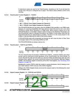
15.10.3 Timer/Counter1 Control Register C – TCCR1C
Bit
7
6
5
–
4
–
3
–
2
–
1
–
0
–
FOC1A
FOC1B
TCCR1C
Read/Write
Initial Value
R/W
0
R/W
0
R
0
R
0
R
0
R
0
R
0
R
0
• Bit 7 – FOCnA: Force Output Compare for Channel A
• Bit 6 – FOCnB: Force Output Compare for Channel B
The FOCnA/FOCnB bits are only active when the WGMn3:0 bits specifies a non-PWM mode.
However, for ensuring compatibility with future devices, these bits must be set to zero when
TCCRnA is written when operating in a PWM mode. When writing a logical one to the
FOCnA/FOCnB bit, an immediate compare match is forced on the Waveform Generation unit.
The OCnA/OCnB output is changed according to its COMnx1:0 bits setting. Note that the
FOCnA/FOCnB bits are implemented as strobes. Therefore it is the value present in the
COMnx1:0 bits that determine the effect of the forced compare.
A FOCnA/FOCnB strobe will not generate any interrupt nor will it clear the timer in Clear Timer
on Compare match (CTC) mode using OCRnA as TOP.
The FOCnA/FOCnB bits are always read as zero.
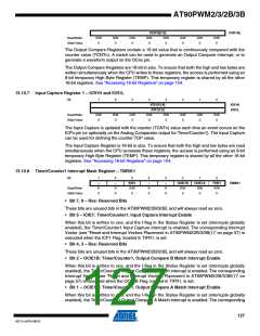
15.10.4 Timer/Counter1 – TCNT1H and TCNT1L
Bit
7
6
5
4
3
2
1
0
TCNT1[15:8]
TCNT1[7:0]
TCNT1H
TCNT1L
Read/Write
Initial Value
R/W
R/W
0
R/W
0
R/W
R/W
0
R/W
0
R/W
0
R/W
0
0
0
The two Timer/Counter I/O locations (TCNTnH and TCNTnL, combined TCNTn) give direct
access, both for read and for write operations, to the Timer/Counter unit 16-bit counter. To
ensure that both the high and low bytes are read and written simultaneously when the CPU
accesses these registers, the access is performed using an 8-bit temporary High Byte Register
(TEMP). This temporary register is shared by all the other 16-bit registers. See “Accessing 16-bit
Registers” on page 104.
Modifying the counter (TCNTn) while the counter is running introduces a risk of missing a com-
pare match between TCNTn and one of the OCRnx Registers.
Writing to the TCNTn Register blocks (removes) the compare match on the following timer clock
for all compare units.
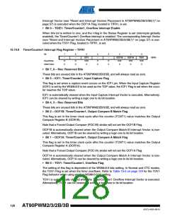
15.10.5 Output Compare Register 1 A – OCR1AH and OCR1AL
Bit
7
6
5
4
3
2
1
0
OCR1A[15:8]
OCR1A[7:0]
OCR1AH
OCR1AL
Read/Write
Initial Value
R/W
R/W
R/W
R/W
R/W
R/W
0
R/W
0
R/W
0
0
0
0
0
0
15.10.6 Output Compare Register 1 B – OCR1BH and OCR1BL
Bit
7
6
5
4
3
2
1
0
OCR1B[15:8]
OCR1BH
126
AT90PWM2/3/2B/3B
4317J–AVR–08/10

 ATMEL [ ATMEL ]