AT90PWM2/3/2B/3B
I/O pin it is connected to. However, note that the Data Direction Register (DDR) bit correspond-
ing to the OCnA or OCnB pin must be set in order to enable the output driver.
When the OCnA or OCnB is connected to the pin, the function of the COMnx1:0 bits is depen-
dent of the WGMn3:0 bits setting. Table 15-2 shows the COMnx1:0 bit functionality when the
WGMn3:0 bits are set to a Normal or a CTC mode (non-PWM).
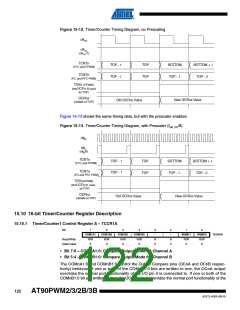
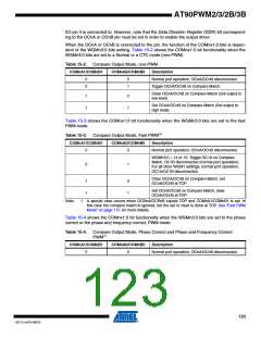
Table 15-2. Compare Output Mode, non-PWM
COMnA1/COMnB1
COMnA0/COMnB0
Description
0
0
0
1
Normal port operation, OCnA/OCnB disconnected.
Toggle OCnA/OCnB on Compare Match.
Clear OCnA/OCnB on Compare Match (Set output to
low level).
1
1
0
1
Set OCnA/OCnB on Compare Match (Set output to
high level).
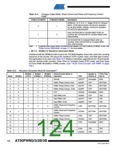
Table 15-3 shows the COMnx1:0 bit functionality when the WGMn3:0 bits are set to the fast
PWM mode.
Table 15-3. Compare Output Mode, Fast PWM(1)
COMnA1/COMnB1
COMnA0/COMnB0
Description
0
0
Normal port operation, OCnA/OCnB disconnected.
WGMn3:0 = 14 or 15: Toggle OC1A on Compare
Match, OC1B disconnected (normal port operation).
For all other WGM1 settings, normal port operation,
OC1A/OC1B disconnected.
0
1
Clear OCnA/OCnB on Compare Match, set
OCnA/OCnB at TOP
1
1
0
1
Set OCnA/OCnB on Compare Match, clear
OCnA/OCnB at TOP
Note:
1. A special case occurs when OCRnA/OCRnB equals TOP and COMnA1/COMnB1 is set. In
this case the compare match is ignored, but the set or clear is done at TOP. See “Fast PWM
Mode” on page 115. for more details.
Table 15-4 shows the COMnx1:0 bit functionality when the WGMn3:0 bits are set to the phase
correct or the phase and frequency correct, PWM mode.
Table 15-4. Compare Output Mode, Phase Correct and Phase and Frequency Correct
PWM(1)
COMnA1/COMnB1
COMnA0/COMnB0
Description
0
0
Normal port operation, OCnA/OCnB disconnected.
123
4317J–AVR–08/10

 ATMEL [ ATMEL ]