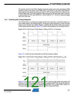
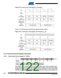
Figure 15-12. Timer/Counter Timing Diagram, no Prescaling
clkI/O
clkTn
(clkI/O/1)
TCNTn
TOP - 1
TOP - 1
TOP
TOP
BOTTOM
TOP - 1
BOTTOM + 1
TOP - 2
(CTC and FPWM)
TCNTn
(PC and PFC PWM)
TOVn (FPWM)
and ICFn (if used
as TOP)
OCRnx
(Update at TOP)
New OCRnx Value
Old OCRnx Value
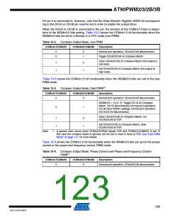
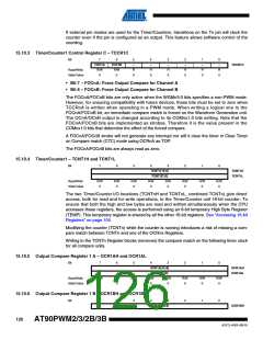
Figure 15-13 shows the same timing data, but with the prescaler enabled.
Figure 15-13. Timer/Counter Timing Diagram, with Prescaler (fclk_I/O/8)
clk
I/O
clk
Tn
(clk /8)
I/O
TCNTn
TOP - 1
TOP - 1
TOP
TOP
BOTTOM
TOP - 1
BOTTOM + 1
TOP - 2
(CTC and FPWM)
TCNTn
(PC and PFC PWM)
TOVn(FPWM)
and ICFn(if used
as TOP)
OCRnx
(Update at TOP)
Old OCRnx Value
New OCRnx Value
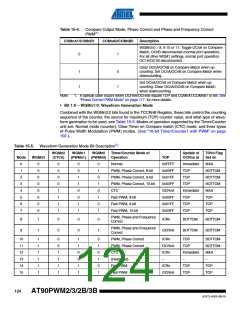
15.10 16-bit Timer/Counter Register Description
15.10.1 Timer/Counter1 Control Register A – TCCR1A
Bit
7
COM1A1
R/W
6
COM1A0
R/W
5
COM1B1
R/W
4
3
–
2
–
1
WGM11
R/W
0
0
WGM10
R/W
0
COM1B0
R/W
0
TCCR1A
Read/Write
Initial Value
R
0
R
0
0
0
0
• Bit 7:6 – COMnA1:0: Compare Output Mode for Channel A
• Bit 5:4 – COMnB1:0: Compare Output Mode for Channel B
The COMnA1:0 and COMnB1:0 control the Output Compare pins (OCnA and OCnB respec-
tively) behavior. If one or both of the COMnA1:0 bits are written to one, the OCnA output
overrides the normal port functionality of the I/O pin it is connected to. If one or both of the
COMnB1:0 bit are written to one, the OCnB output overrides the normal port functionality of the
122
AT90PWM2/3/2B/3B
4317J–AVR–08/10

 ATMEL [ ATMEL ]