AT89S8252
Programming the
Flash and EEPROM
Atmel’s AT89S8252 Flash Microcontroller offers 8K bytes of in-system reprogrammable
Flash Code memory and 2K bytes of EEPROM Data memory.
The AT89S8252 is normally shipped with the on-chip Flash Code and EEPROM Data
memory arrays in the erased state (i.e. contents = FFH) and ready to be programmed.
This device supports a High-voltage (12-V VPP) Parallel programming mode and a Low-
voltage (5-V VCC) Serial programming mode. The serial programming mode provides a
convenient way to reprogram the AT89S8252 inside the user’s system. The parallel pro-
gramming mode is compatible with conventional third party Flash or EPROM
programmers.
The Code and Data memory arrays are mapped via separate address spaces in the
serial programming mode. In the parallel programming mode, the two arrays occupy
one contiguous address space: 0000H to 1FFFH for the Code array and 2000H to
27FFH for the Data array.
The Code and Data memory arrays on the AT89S8252 are programmed byte-by-byte in
either programming mode. An auto-erase cycle is provided with the self-timed program-
ming operation in the serial programming mode. There is no need to perform the Chip
Erase operation to reprogram any memory location in the serial programming mode
unless any of the lock bits have been programmed.
In the parallel programming mode, there is no auto-erase cycle. To reprogram any non-
blank byte, the user needs to use the Chip Erase operation first to erase both arrays.
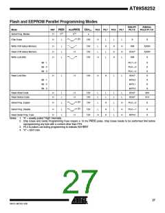
Parallel Programming Algorithm: To program and verify the AT89S8252 in the paral-
lel programming mode, the following sequence is recommended:
1. Power-up sequence:
Apply power between VCC and GND pins.
Set RST pin to “H”.
Apply a 3 MHz to 24 MHz clock to XTAL1 pin and wait for at least 10 milliseconds.
2. Set PSEN pin to “L”
ALE pin to “H”
EA pin to “H” and all other pins to “H”.
3. Apply the appropriate combination of “H” or “L” logic levels to pins P2.6, P2.7, P3.6,
P3.7 to select one of the programming operations shown in the Flash Programming
Modes table.
4. Apply the desired byte address to pins P1.0 to P1.7 and P2.0 to P2.5.
Apply data to pins P0.0 to P0.7 for Write Code operation.
5. Raise EA/VPP to 12V to enable Flash programming, erase or verification.
6. Pulse ALE/PROG once to program a byte in the Code memory array, the Data mem-
ory array or the lock bits. The byte-write cycle is self-timed and typically takes
1.5 ms.
7. To verify the byte just programmed, bring pin P2.7 to “L” and read the programmed
data at pins P0.0 to P0.7.
8. Repeat steps 3 through 7 changing the address and data for the entire 2K or 8K
bytes array or until the end of the object file is reached.
9. Power-off sequence:
Set XTAL1 to “L”.
Set RST and EA pins to “L”.
Turn VCC power off.
23
0401G–MICRO–3/06

 ATMEL [ ATMEL ]