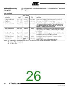
AT89S8252
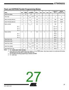
Flash and EEPROM Parallel Programming Modes
Data I/O
P0.7:0
Address
P2.5:0 P1.7:0
Mode
RST
PSEN
ALE/PROG
EA/VPP
P2.6
P2.7
P3.6
P3.7
Serial Prog. Modes
H
h(1)
h(1)
x
(2)
Chip Erase
H
L
12V
H
L
L
L
X
X
Write (10K bytes) Memory
Read (10K bytes) Memory
Write Lock Bits:
H
H
H
L
L
L
12V
12V
12V
L
L
H
L
L
H
H
H
H
H
L
DIN
DOUT
DIN
ADDR
ADDR
X
H
H
Bit - 1
Bit - 2
Bit - 3
P0.7 = 0
P0.6 = 0
P0.5 = 0
DOUT
X
X
X
Read Lock Bits:
H
L
H
12V
H
H
L
L
X
Bit - 1
Bit - 2
Bit - 3
@P0.2
@P0.1
@P0.0
DOUT
X
X
X
Read Atmel Code
Read Device Code
H
H
L
L
H
H
12V
12V
L
L
L
L
L
L
L
L
30H
31H
DOUT
(2)
Serial Prog. Enable
H
L
12V
L
H
L
H
P0.0 = 0
X
(2)
Serial Prog. Disable
H
H
L
L
12V
12V
L
H
H
L
L
H
H
P0.0 = 1
@P0.0
X
X
Read Serial Prog. Fuse
H
H
Notes: 1. “h” = weakly pulled “High” internally.
2. Chip Erase and Serial Programming Fuse require a 10 ms PROG pulse. Chip Erase needs to be performed first before
reprogramming any byte with a content other than FFH.
3. P3.4 is pulled Low during programming to indicate RDY/BSY.
4. “X” = don’t care
27
0401G–MICRO–3/06

 ATMEL [ ATMEL ]