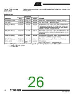
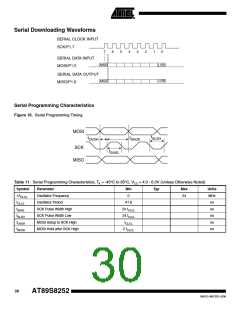
Serial Programming
Instruction
The Instruction Set for Serial Programming follows a 3-byte protocol and is shown in the
following table:
Instruction Set
Input Format
Instruction
Byte 1
Byte 2
0101 0011
xxxx x100
low addr
Byte 3
Operation
Programming Enable
Chip Erase
1010 1100
1010 1100
aaaa a001
xxxx xxxx
xxxx xxxx
xxxx xxxx
Enable serial programming interface after RST goes high.
Chip erase both 8K & 2K memory arrays.
Read Code Memory
Read data from Code memory array at the selected address.
The 5 MSBs of the first byte are the high order address bits.
The low order address bits are in the second byte. Data are
available at pin MISO during the third byte.
Write Code Memory
Read Data Memory
aaaa a010
00aa a101
low addr
low addr
data in
Write data to Code memory location at selected address. The
address bits are the 5 MSBs of the first byte together with the
second byte.
xxxx xxxx
Read data from Data memory array at selected address. Data
are available at pin MISO during the third byte.
Write Data Memory
Write Lock Bits
00aa a110
1010 1100
low addr
x x111
data in
Write data to Data memory location at selected address.
xxxx xxxx
Write lock bits.
Set LB1, LB2 or LB3 = “0” to program lock bits.
Notes: 1. DATA polling is used to indicate the end of a byte write cycle which typically takes less than 2.5 ms at 5V.
2. “aaaaa” = high order address.
3. “x” = don’t care.
26
AT89S8252
0401G–MICRO–3/06

 ATMEL [ ATMEL ]