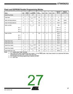
In the parallel programming mode, there is no auto-erase cycle and to reprogram any
non-blank byte, the user needs to use the Chip Erase operation first to erase both
arrays.
Data Polling: The AT89S8252 features DATA Polling to indicate the end of a byte write
cycle. During a byte write cycle in the parallel or serial programming mode, an
attempted read of the last byte written will result in the complement of the written datum
on P0.7 (parallel mode), and on the MSB of the serial output byte on MISO (serial
mode). Once the write cycle has been completed, true data are valid on all outputs, and
the next cycle may begin. DATA Polling may begin any time after a write cycle has been
initiated.
Ready/Busy: The progress of byte programming in the parallel programming mode can
also be monitored by the RDY/BSY output signal. Pin P3.4 is pulled Low after ALE goes
High during programming to indicate BUSY. P3.4 is pulled High again when program-
ming is done to indicate READY.
Program Verify: If lock bits LB1 and LB2 have not been programmed, the programmed
Code or Data byte can be read back via the address and data lines for verification. The
state of the lock bits can also be verified directly in the parallel programming mode. In
the serial programming mode, the state of the lock bits can only be verified indirectly by
observing that the lock bit features are enabled.
Chip Erase: Both Flash and EEPROM arrays are erased electrically at the same time.
In the parallel programming mode, chip erase is initiated by using the proper combina-
tion of control signals and by holding ALE/PROG low for 10 ms. The Code and Data
arrays are written with all “1”s in the Chip Erase operation.
In the serial programming mode, a chip erase operation is initiated by issuing the Chip
Erase instruction. In this mode, chip erase is self-timed and takes about 16 ms.
During chip erase, a serial read from any address location will return 00H at the data
outputs.
Serial Programming Fuse: A programmable fuse is available to disable Serial Pro-
gramming if the user needs maximum system security. The Serial Programming Fuse
can only be programmed or erased in the Parallel Programming Mode.
The AT89S8252 is shipped with the Serial Programming Mode enabled.
Reading the Signature Bytes: The signature bytes are read by the same procedure as
a normal verification of locations 030H and 031H, except that P3.6 and P3.7 must be
pulled to a logic low. The values returned are as follows:
(030H) = 1EH indicates manufactured by Atmel
(031H) = 72H indicates 89S8252
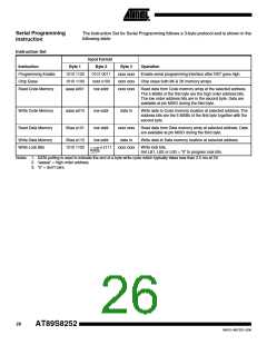
Programming
Interface
Every code byte in the Flash and EEPROM arrays can be written, and the entire array
can be erased, by using the appropriate combination of control signals. The write opera-
tion cycle is self-timed and once initiated, will automatically time itself to completion.
Most worldwide major programming vendors offer support for the Atmel AT89 microcon-
troller series. Please contact your local programming vendor for the appropriate
software revision.
24
AT89S8252
0401G–MICRO–3/06

 ATMEL [ ATMEL ]