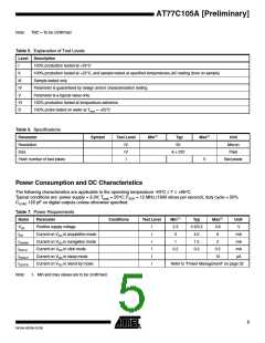
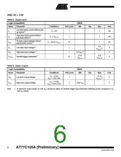
VDD_IO = 1.8V
Table 8. Digital Inputs
Logic Compatibility
CMOS
Min
Name
Parameter
Conditions
Test Level
Typ
Max
Unit
Low level input current without pull-
up device(1)
IIL
VI = 0V
I
1
µA
High level input current without
pull-down device(1)
IIH
VI = VDD_IO
I
1
1
µA
µA
Tri-state output leakage without
pull-up/down device(1)
IIOZ
VI = 0V or VDD_IO
IV
0.4
VDD_IO
VIL
Low level input voltage(1)
High level input voltage(1)
Schmitt trigger hysteresis(1)
I
I
V
V
V
(1)
(1)
VIH
0.6 VDD
0.15
0.3
VDD_IO
VHYST
IV
VDD_IO
Table 9. Digital Outputs
Logic Compatibility
CMOS
Min
Name
Parameter
Conditions
Test Level
Typ
Max
Unit
IOL = 4 mA
VDD = 1.8V 8%
0.15
VDD_IO
VOL
Low level output voltage
I
V
(1)
I
OH = -4 mA
VOH
High level output voltage
I
0.85 VDD
V
VDD = 3.3V 10%
Note:
1. A minimum noise margin of 0.05 VDD should be taken for Schmitt trigger input threshold switching levels compared to VIL
and VIH values.
6
AT77C105A [Preliminary]
5419A–BIOM–01/05

 ATMEL [ ATMEL ]