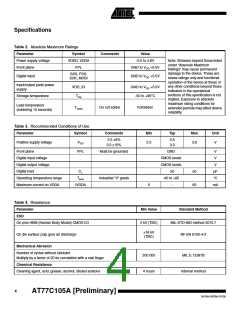
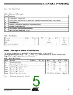
Specifications
Table 2. Absolute Maximum Ratings
Parameter
Symbol
Comments
Value
Power supply voltage
Front plane
VDDD, VDDA
FPL
-0.5 to 4.6V
Note: Stresses beyond those listed
under “Absolute Maximum
GND to VDD +0.5V
Ratings” may cause permanent
damage to the device. These are
stress ratings only and functional
operation of the device at these or
any other conditions beyond those
indicated in the operational
sections of this specification is not
implied. Exposure to absolute
maximum rating conditions for
extended periods may affect device
reliability.
SSS, FSS,
SCK, MOSI
Digital input
GND to VDD +0.5V
Input/output pads power
supply
VDD_IO
Tstg
GND to VDD +0.5V
Storage temperature
-50 to +95°C
Lead temperature
(soldering 10 seconds)
Tleads
Do not solder
Forbidden
Table 3. Recommended Conditions of Use
Parameter
Symbol
Comments
Min
Typ
Max
Unit
2.5 5%
2.5
3.3
Positive supply voltage
VDD
2.3
3.6
V
3.3 10%
Front plane
FPL
Must be grounded
GND
CMOS levels
CMOS levels
20
V
V
Digital input voltage
Digital output voltage
Digital load
V
CL
50
60
pF
°C
mA
Operating temperature range
Maximum current on VDDA
Tamb
Industrial “V” grade
-40 to +85
-
IVDDA
0
Table 4. Resistance
Parameter
Min Value
Standard Method
ESD
On pins HBM (Human Body Model) CMOS I/O
2 kV (TBC)
MIL-STD-883 method 3015.7
NF EN 6100-4-2
16 kV
(TBC)
On die surface (zap gun) air discharge
Mechanical Abrasion
Number of cycles without lubricant
200 000
4 hours
MIL E 12397B
Multiply by a factor of 20 for correlation with a real finger
Chemical Resistance
Cleaning agent, acid, grease, alcohol, diluted acetone
Internal method
4
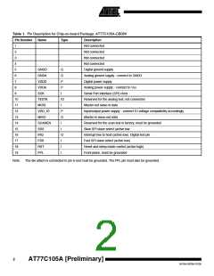
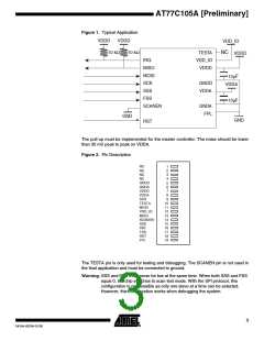
AT77C105A [Preliminary]
5419A–BIOM–01/05

 ATMEL [ ATMEL ]