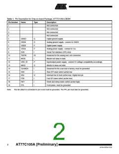
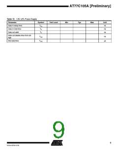
AT77C105A [Preliminary]
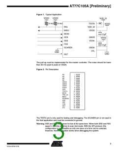
Figure 1. Typical Application
VDDD VDDD
VDD_IO
10 kΩ
10 kΩ
NC
TESTA
VDD_IO
VDDD
VDDD
IRQ
MISO
MOSI
SCK
F
10µ
GNDD
VDDA
VDDA
SSS
FSS
10µF
SCANEN
GNDA
FPL
GND
GND
RST
The pull-up must be implemented for the master controller. The noise should be lower
than 30 mV peak to peak on VDDA.
Figure 2. Pin Description
NC
NC
1
2
NC
3
NC
4
GNDD
GNDA
VDDD
VDDA
SCK
5
6
7
8
9
TESTA
MOSI
VDD_IO
MISO
SCANEN
SSS
IRQ
FSS
RST
FPL
10
11
12
13
14
15
16
17
18
19
The TESTA pin is only used for testing and debugging. The SCANEN pin is not used in
the final application and must be connected to ground.
Warning: SSS and FSS must never be low at the same time. When both SSS and FSS
equal 0, the chip switches to scan test mode. With the SPI protocol, this
configuration is not possible as only one slave at a time can be selected.
However, this configuration works when debugging the system.
3
5419A–BIOM–01/05

 ATMEL [ ATMEL ]