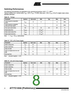
Switching Performances
The following characteristics are applicable to the operating temperature -40°C ≤ T ≤ +85°C.
Typical conditions are: nominal value; Tamb = 25°C; FSCK = 12 MHz; duty cycle = 50%; CLOAD 120 pF in digital output unless
specified otherwise.
Table 12. Timings
Parameter
Symbol
Test Level
Min
Typ
Max
Unit
Clock frequency acquisition
mode
FACQ
IV
8
16
MHz
Clock frequency navigation
mode and chip control
FCTRL
I
-
0.2
80
MHz
Duty cycle (clock SCK)
Reset setup time
DC
IV
I
20
50
%
ns
ns
ns
(1)
(1)
(1)
TRSTSU
TSSSU
TSSHD
½ TSCK
½ TSCK
½ TSCK
Slave select setup time
Slave select hold time
I
I
Note:
1. TSCK = 1/FCTRL (clock period)
Table 13. 3.3V 10% Power Supply
Parameter
Symbol
TSU
Test Level
Min
Typ
3
Max
Unit
ns
Data in setup time
IV
IV
I
Data in hold time
TH
1
ns
Data out valid
TV
30
3
ns
Data out disable time from SS
high
TDIS
TIRQ
IV
IV
3.8
ns
µs
IRQ hold time
Note:
All power supplies = +3.3V
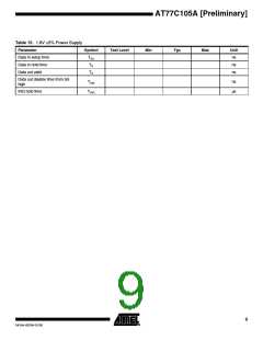
Table 14. 2.5V 5% Power Supply
Parameter
Symbol
TSU
Test Level
Min
Typ
3
Max
Unit
ns
Data in setup time
Data in hold time
IV
IV
I
TH
1
ns
Data out valid
TV
30
3
ns
Data out disable time from SS
high
TDIS
TIRQ
IV
IV
3.8
ns
µs
IRQ hold time
Note:
All power supplies = +2.5V
8
AT77C105A [Preliminary]
5419A–BIOM–01/05

 ATMEL [ ATMEL ]