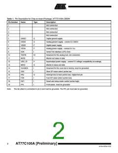
Table 1. Pin Description for Chip-on-board Package: AT77C105A-CB08V
Pin Number
Name
Type
Description
1
Not connected
2
Not connected
3
Not connected
4
Not connected
5
GNDD
GNDA
VDDD
VDDA
SCK
G
G
P
P
I
Digital ground supply
6
Analog ground supply - connect to GNDD
Digital power supply
7
8
Analog power supply - connect to VDD
Serial Port Interface (SPI) clock
Reserved for the analog test, not connected
Master-out slave-in data
9
10
11
12
13
14
15
16
17
18
19
TESTA
MOSI
VDD_IO
MISO
SCANEN
SSS
IO
I
P
O
I
Input/output power supply - connect IO voltage compatibility accordingly
Master-in slave-out data
Reserved for the scan test in factory, must be grounded
Slow SPI slave select (active low
Interrupt line to host (active low). Digital test pin
Fast SPI slave select (active low)
Reset and sleep mode control (active high)
Front plane, must be grounded
I
IRQ
O
I
FSS
RST
I
FPL
I
Note:
The die attach is connected to pin 6 and must be grounded. The FPL pin must also be grounded.
2
AT77C105A [Preliminary]
5419A–BIOM–01/05

 ATMEL [ ATMEL ]