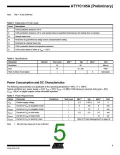
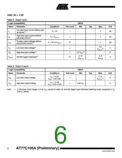
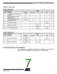
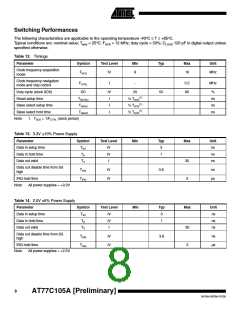
AT77C105A [Preliminary]
Note:
TBC = To be confirmed
Table 5. Explanation of Test Levels
Level Description
I
100% production tested at +25°C
II
100% production tested at +25°C, and sample tested at specified temperatures (AC testing done on sample)
Sample tested only
III
IV
V
VI
D
Parameter is guaranteed by design and/or characterization testing
Parameter is a typical value only
100% production tested at temperature extremes
100% probe tested on wafer at Tamb = +25°C
Table 6. Specifications
Parameter
Symbol
Test Level
Min(1)
Typ
50
Max(1)
Unit
Micron
Pixel
Resolution
IV
IV
I
Size
8 × 232
Yield: number of bad pixels
5
Bad pixels
Power Consumption and DC Characteristics
The following characteristics are applicable to the operating temperature -40°C ≤ T ≤ +85°C.
Typical conditions are: power supply = 3.3V; Tamb = 25°C; FSCK = 12 MHz (1600 slices per second); duty cycle = 50%
LOAD 120 pF on digital outputs unless otherwise specified.
C
Table 7. Power Requirements
Name
VDD
Parameter
Conditions
Test Level
Min(1)
2.3
3
Typ
2.5/3.3
4.5
Max(1)
3.6
6
Unit-
V
Positive supply voltage
I
I
I
I
I
I
IDD
Current on VDD in acquisition mode
Current on VDD in navigation mode
Current on VDD in click mode
Current on VDD in sleep mode
Current on VDD in stand-by mode
mA
mA
mA
µA
IDDNAV
IDDCLI
IDDSLP
IDDSTB
1
1.5
2
0.2
0.3
0.5
10
Refer to “Power Management” on page 32
Note:
1. Min and max values are to be confirmed.
5
5419A–BIOM–01/05

 ATMEL [ ATMEL ]