BUFFER TO MAIN MEMORY PAGE PROGRAM WITHOUT BUILT-IN ERASE: A previously
erased page within main memory can be programmed with the contents of the buffer. An 8-bit
opcode of 88H is followed by the six reserved bits, nine address bits (PA8-PA0) that specify
the page in the main memory to be written, and nine additional don’t care bits. When a low-to-
high transition occurs on the CS pin, the part will program the data stored in the buffer into the
specified page in the main memory. It is necessary that the page in main memory that is being
programmed has been previously erased. The programming of the page is internally self-
timed and should take place in a maximum time of tP. During this time, the status register will
indicate that the part is busy.
Successive page programming operations without doing a page erase are not recommended.
In other words, changing bytes within a page from a “1” to a “0” during multiple page program-
ming operations without erasing that page is not recommended.
PAGE ERASE: The optional Page Erase command can be used to individually erase any
page in the main memory array allowing the Buffer to Main Memory Page Program without
Built-in Erase command to be utilized at a later time. To perform a Page Erase, an opcode of
81H must be loaded into the device, followed by six reserved bits, nine address bits (PA8-
PA0), and nine don’t care bits. The nine address bits are used to specify which page of the
memory array is to be erased. When a low-to-high transition occurs on the CS pin, the part will
erase the selected page to 1s. The erase operation is internally self-timed and should take
place in a maximum time of tPE. During this time, the status register will indicate that the part is
busy.
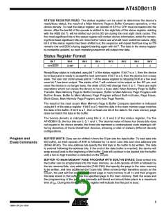
BLOCK ERASE: A block of eight pages can be erased at one time allowing the Buffer to Main
Memory Page Program without Built-in Erase command to be utilized to reduce programming
times when writing large amounts of data to the device. To perform a Block Erase, an opcode
of 50H must be loaded into the device, followed by six reserved bits, six address bits (PA8-
PA3), and 12 don’t care bits. The six address bits are used to specify which block of eight
pages is to be erased. When a low-to-high transition occurs on the CS pin, the part will erase
the selected block of eight pages to 1s. The erase operation is internally self-timed and should
take place in a maximum time of tBE. During this time, the status register will indicate that the
part is busy.
Block Erase Addressing
PA8
PA7
PA6
PA5
PA4
0
PA3
0
PA2
X
PA1
X
PA0
X
Block
0
0
0
0
0
1
2
3
0
0
0
0
0
1
X
X
X
0
0
0
0
1
0
X
X
X
0
0
0
0
1
1
X
X
X
•
•
•
•
•
•
•
•
•
•
•
•
•
•
•
•
•
•
•
•
•
•
•
•
•
•
•
•
•
•
1
1
1
1
1
1
1
1
1
1
1
1
1
1
1
1
0
0
1
1
0
1
0
1
X
X
X
X
X
X
X
X
X
X
X
X
60
61
62
63
6
AT45DB011B
1984H–DFLSH–10/04

 ATMEL [ ATMEL ]