AT45DB011B
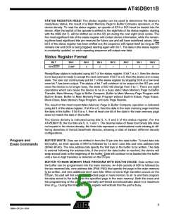
STATUS REGISTER READ: The status register can be used to determine the device’s
ready/busy status, the result of a Main Memory Page to Buffer Compare operation, or the
device density. To read the status register, an opcode of 57H or D7H must be loaded into the
device. After the last bit of the opcode is shifted in, the eight bits of the status register, starting
with the MSB (bit 7), will be shifted out on the SO pin during the next eight clock cycles. The
five most significant bits of the status register will contain device information, while the remain-
ing three least significant bits are reserved for future use and will have undefined values. After
bit 0 of the status register has been shifted out, the sequence will repeat itself (as long as CS
remains low and SCK is being toggled) starting again with bit 7. The data in the status register
is constantly updated, so each repeating sequence will output new data.
Status Register Format
Bit 7
Bit 6
Bit 5
Bit 4
Bit 3
Bit 2
Bit 1
Bit 0
RDY/BUSY
COMP
0
0
1
1
X
X
Ready/Busy status is indicated using bit 7 of the status register. If bit 7 is a 1, then the device
is not busy and is ready to accept the next command. If bit 7 is a 0, then the device is in a busy
state. The user can continuously poll bit 7 of the status register by stopping SCK at a low level
once bit 7 has been output. The status of bit 7 will continue to be output on the SO pin, and
once the device is no longer busy, the state of SO will change from 0 to 1. There are eight
operations which can cause the device to be in a busy state: Main Memory Page to Buffer
Transfer, Main Memory Page to Buffer Compare, Buffer to Main Memory Page Program with
Built-in Erase, Buffer to Main Memory Page Program without Built-in Erase, Page Erase,
Block Erase, Main Memory Page Program, and Auto Page Rewrite.
The result of the most recent Main Memory Page to Buffer Compare operation is indicated
using bit 6 of the status register. If bit 6 is a 0, then the data in the main memory page matches
the data in the buffer. If bit 6 is a 1, then at least one bit of the data in the main memory page
does not match the data in the buffer.
The device density is indicated using bits 5, 4, 3 and 2 of the status register. For the
AT45DB011B, the four bits are 0, 0, 1 and 1. The decimal value of these four binary bits does
not equate to the device density; the three bits represent a combinational code relating to dif-
fering densities of Serial DataFlash devices, allowing a total of sixteen different density
configurations.
Program and
Erase Commands
BUFFER WRITE: Data can be shifted in from the SI pin into the data buffer. To load data into
the buffer, an 8-bit opcode of 84H is followed by 15 don’t care bits and nine address bits
(BFA8-BFA0). The nine address bits specify the first byte in the buffer to be written. The data
is entered following the address bits. If the end of the data buffer is reached, the device will
wrap around back to the beginning of the buffer. Data will continue to be loaded into the buffer
until a low-to-high transition is detected on the CS pin.
BUFFER TO MAIN MEMORY PAGE PROGRAM WITH BUILT-IN ERASE: Data written into
the buffer can be programmed into the main memory. An 8-bit opcode of 83H is followed by
the six reserved bits, nine address bits (PA8-PA0) that specify the page in the main memory
to be written, and nine additional don’t care bits. When a low-to-high transition occurs on the
CS pin, the part will first erase the selected page in main memory to all 1s and then program
the data stored in the buffer into the specified page in the main memory. Both the erase and
the programming of the page are internally self-timed and should take place in a maximum
time of tEP. During this time, the status register will indicate that the part is busy.
5
1984H–DFLSH–10/04

 ATMEL [ ATMEL ]