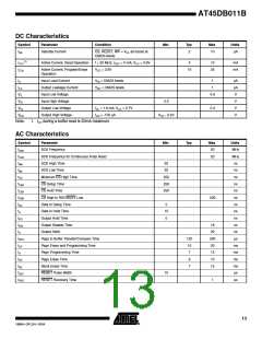
AT45DB011B
Operation Mode
Summary
The modes described can be separated into two groups – modes which make use of the Flash
memory array (Group A) and modes which do not make use of the Flash memory array
(Group B).
Group A modes consist of:
1. Main Memory Page Read
2. Main Memory Page to Buffer Transfer
3. Main Memory Page to Buffer Compare
4. Buffer to Main Memory Page Program with Built-in Erase
5. Buffer to Main Memory Page Program without Built-in Erase
6. Page Erase
7. Block Erase
8. Main Memory Page Program through Buffer
9. Auto Page Rewrite
Group B modes consist of:
1. Buffer Read
2. Buffer Write
3. Status Register Read
If a Group A mode is in progress (not fully completed), then another mode in Group A should
not be started. However, during this time in which a Group A mode is in progress (other than
Main Memory Page Read), Status Register Read from Group B can be started. Furthermore,
during Page Erase and Block Erase operation in progress from Group A, any of the modes
from Group B can be started.
Pin Descriptions
SERIAL INPUT (SI): The SI pin is an input-only pin and is used to shift data into the device.
The SI pin is used for all data input, including opcodes and address sequences.
SERIAL OUTPUT (SO): The SO pin is an output-only pin and is used to shift data out from the
device.
SERIAL CLOCK (SCK): The SCK pin is an input-only pin and is used to control the flow of
data to and from the DataFlash. Data is always clocked into the device on the rising edge of
SCK and clocked out of the device on the falling edge of SCK.
CHIP SELECT (CS): The DataFlash is selected when the CS pin is low. When the device is
not selected, data will not be accepted on the SI pin, and the SO pin will remain in a high-
impedance state. A high-to-low transition on the CS pin is required to start an operation, and a
low-to-high transition on the CS pin is required to end an operation.
WRITE PROTECT: If the WP pin is held low, the first 256 pages of the main memory cannot
be reprogrammed. The only way to reprogram the first 256 pages is to first drive the protect
pin high and then use the program commands previously mentioned. If this pin and feature are
not utilized it is recommended that the WP pin be driven high externally.
9
1984H–DFLSH–10/04

 ATMEL [ ATMEL ]