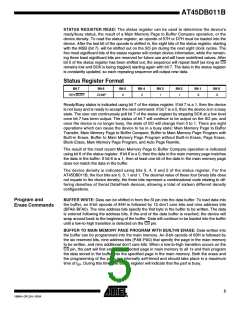
layout, increases system reliability, minimizes switching noise, and reduces package size and
active pin count. The device is optimized for use in many commercial and industrial applica-
tions where high density, low pin count, low voltage, and low power are essential. The device
operates at clock frequencies up to 20 MHz with a typical active read current consumption of
4 mA.
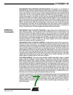
To allow for simple in-system reprogrammability, the AT45DB011B does not require high input
voltages for programming. The device operates from a single power supply, 2.7V to 3.6V, for
both the program and read operations. The AT45DB011B is enabled through the chip select
pin (CS) and accessed via a three-wire interface consisting of the Serial Input (SI), Serial Out-
put (SO), and the Serial Clock (SCK).
All programming cycles are self-timed, and no separate erase cycle is required before
programming.
When the device is shipped from Atmel, the most significant page of the memory array may
not be erased. In other words, the contents of the last page may not be filled with FFH.
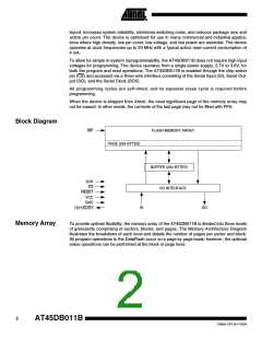
Block Diagram
WP
FLASH MEMORY ARRAY
PAGE (264 BYTES)
BUFFER (264 BYTES)
I/O INTERFACE
SCK
CS
RESET
VCC
GND
RDY/BUSY
SI
SO
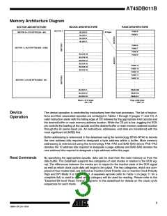
Memory Array
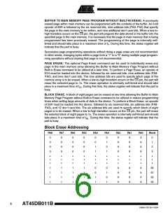
To provide optimal flexibility, the memory array of the AT45DB011B is divided into three levels
of granularity comprising of sectors, blocks, and pages. The Memory Architecture Diagram
illustrates the breakdown of each level and details the number of pages per sector and block.
All program operations to the DataFlash occur on a page by page basis; however, the optional
erase operations can be performed at the block or page level.
2
AT45DB011B
1984H–DFLSH–10/04

 ATMEL [ ATMEL ]