AT45DB011B
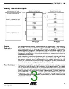
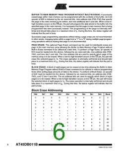
Memory Architecture Diagram
SECTOR ARCHITECTURE
BLOCK ARCHITECTURE
PAGE ARCHITECTURE
SECTOR 0
PAGE 0
PAGE 1
8 Pages
SECTOR 0 = 2112 BYTES (2K + 64)
BLOCK 0
BLOCK 1
BLOCK 2
BLOCK 3
PAGE 6
PAGE 7
PAGE 8
PAGE 9
SECTOR 1 = 65,472 BYTES (62K + 1984)
BLOCK 29
BLOCK 30
BLOCK 31
BLOCK 32
BLOCK 33
BLOCK 34
PAGE 14
PAGE 15
PAGE 16
PAGE 17
PAGE 18
SECTOR 2 = 67,584 BYTES (64K + 2K)
BLOCK 61
BLOCK 62
BLOCK 63
PAGE 509
PAGE 510
PAGE 511
Block = 2112 bytes
(2K + 64)
Page = 264 bytes
(256 + 8)
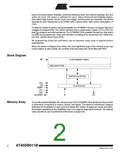
Device
Operation
The device operation is controlled by instructions from the host processor. The list of instruc-
tions and their associated opcodes are contained in Tables 1 through 4 (pages 11 and 12). A
valid instruction starts with the falling edge of CS followed by the appropriate 8-bit opcode and
the desired buffer or main memory address location. While the CS pin is low, toggling the SCK
pin controls the loading of the opcode and the desired buffer or main memory address location
through the SI (serial input) pin. All instructions, addresses, and data are transferred with the
most significant bit (MSB) first.
Buffer addressing is referenced in the datasheet using the terminology BFA8-BFA0 to denote
the nine address bits required to designate a byte address within a buffer. Main memory
addressing is referenced using the terminology PA8-PA0 and BA8-BA0 where PA8-PA0
denotes the 10 address bits required to designate a page address and BA8-BA0 denotes the
nine address bits required to designate a byte address within the page.
Read Commands
By specifying the appropriate opcode, data can be read from the main memory or from the
data buffer. The DataFlash supports two categories of read modes in relation to the SCK sig-
nal. The differences between the modes are in respect to the inactive state of the SCK signal
as well as which clock cycle data will begin to be output. The two categories, which are com-
prised of four modes total, are defined as Inactive Clock Polarity Low or Inactive Clock Polarity
High and SPI Mode 0 or SPI Mode 3. A separate opcode (refer to Table 1 on page 11 for a
complete list) is used to select which category will be used for reading. Please refer to the
“Detailed Bit-level Read Timing” diagrams in this datasheet for details on the clock cycle
sequences for each mode.
3
1984H–DFLSH–10/04

 ATMEL [ ATMEL ]