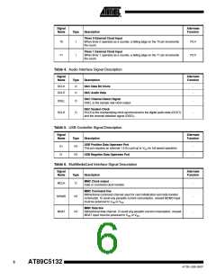
Signal
Name
Alternate
Function
Type
Description
Timer 0 External Clock Input
When timer 0 operates as a counter, a falling edge on the T0 pin increments
the count.
T0
T1
I
P3.4
P3.5
Timer 1 External Clock Input
I
When timer 1 operates as a counter, a falling edge on the T1 pin increments
the count.
Table 4. Audio Interface Signal Description
Signal
Alternate
Function
Name
DCLK
DOUT
Type
O
Description
DAC Data Bit Clock
DAC Audio Data
-
-
O
DAC Channel Select Signal
DSEL
SCLK
O
O
-
-
DSEL is the sample rate clock output.
DAC System Clock
SCLK is the oversampling clock synchronized to the digital audio data (DOUT)
and the channel selection signal (DSEL).
Table 5. USB Controller Signal Description
Signal
Name
Alternate
Function
Type
I/O
Description
USB Positive Data Upstream Port
D+
-
-
This pin requires an external 1.5 KΩ pull-up to VDD for full speed operation.
D-
I/O
USB Negative Data Upstream Port
Table 6. MutiMediaCard Interface Signal Description
Signal
Name
Alternate
Function
Type
Description
MMC Clock output
Data or command clock transfer.
MCLK
O
-
-
MMC Command line
Bidirectional command channel used for card initialization and data transfer
commands. To avoid any parasitic current consumption, unused MCMD input
MCMD
MDAT
I/O
I/O
must be polarized to VDD or VSS
.
MMC Data line
Bidirectional data channel. To avoid any parasitic current consumption, unused
MDAT input must be polarized to VDD or VSS
-
.
6
AT89C5132
4173E–USB–09/07

 ATMEL [ ATMEL ]