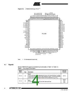
Figure 4-2. AT89C5132 84-pin PLCC (1)
ALE 12
ISP 13
74 NC
73 P4.5
P1.0/KIN0 14
P1.1/KIN1 15
P1.2/KIN2 16
P1.3/KIN3 17
P1.4 18
72 P4.4
71 P2.2/A10
70 P2.3/A11
69 P2.4/A12
68 P2.5/A13
67 P2.6/A14
66 P2.7/A15
65 VSS
P1.5 19
P1.6/SCL 20
P1.7/SDA 21
VDD 22
PLCC84
64 VDD
PAVDD 23
FILT 24
63 MCLK
62 MDAT
61 MCMD
60 RST
PAVSS 25
VSS 26
X2 27
59 SCLK
58 DSEL
57 DCLK
56 DOUT
55 VSS
NC 28
X1 29
TST 30
UVDD 31
UVSS 32
54 VDD
Note:
1. For development board only.
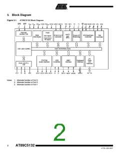
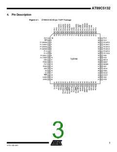
4.1
Signals
All the AT89C5132 signals are detailed by functionality in Table 1 to Table 14.
Table 1. Ports Signal Description
Signal
Name
Alternate
Function
Type
Description
Port 0
P0 is an 8-bit open-drain bidirectional I/O port. Port 0 pins that have 1s written
to them float and can be used as high impedance inputs. To avoid any parasitic
P0.7:0
I/O
AD7:0
current consumption, floating P0 inputs must be polarized to VDD or VSS
.
KIN3:0
SCL
SDA
Port 1
P1 is an 8-bit bidirectional I/O port with internal pull-ups.
P1.7:0
I/O
4
AT89C5132
4173E–USB–09/07

 ATMEL [ ATMEL ]