AT89C5132
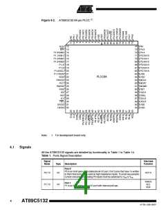
Signal
Name
Alternate
Function
Type
Description
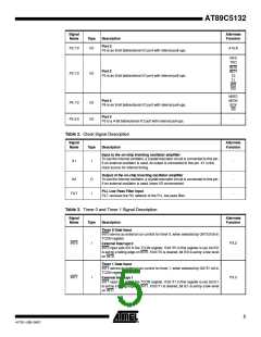
Port 2
P2 is an 8-bit bidirectional I/O port with internal pull-ups.
P2.7:0
I/O
A15:8
RXD
TXD
INT0
INT1
T0
Port 3
P3.7:0
I/O
P3 is an 8-bit bidirectional I/O port with internal pull-ups.
T1
WR
RD
MISO
MOSI
SCK
SS
Port 4
P4.7:0
P5.3:0
I/O
I/O
P4 is an 8-bit bidirectional I/O port with internal pull-ups.
Port 5
P5 is a 4-bit bidirectional I/O port with internal pull-ups.
-
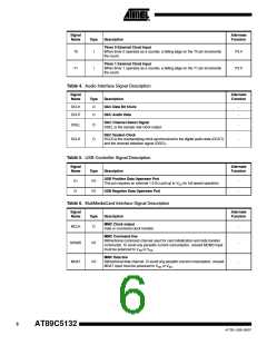
Table 2. Clock Signal Description
Signal
Alternate
Function
Name
Type
Description
Input to the on-chip inverting oscillator amplifier
To use the internal oscillator, a crystal/resonator circuit is connected to this pin.
If an external oscillator is used, its output is connected to this pin. X1 is the
clock source for internal timing.
X1
I
-
Output of the on-chip inverting oscillator amplifier
To use the internal oscillator, a crystal/resonator circuit is connected to this pin.
If an external oscillator is used, leave X2 unconnected.
X2
O
I
-
-
PLL Low Pass Filter input
FILT
FILT receives the RC network of the PLL low pass filter.
Table 3. Timer 0 and Timer 1 Signal Description
Signal
Alternate
Function
Name
Type
Description
Timer 0 Gate Input
INT0 serves as external run control for timer 0, when selected by GATE0 bit in
TCON register.
INT0
I
P3.2
External Interrupt 0
INT0 input sets IE0 in the TCON register. If bit IT0 in this register is set, bit IE0
is set by a falling edge on INT0. If bit IT0 is cleared, bit IE0 is set by a low level
on INT0.
Timer 1 Gate Input
INT1 serves as external run control for timer 1, when selected by GATE1 bit in
TCON register.
INT1
I
P3.3
External Interrupt 1
INT1 input sets IE1 in the TCON register. If bit IT1 in this register is set, bit IE1
is set by a falling edge on INT1. If bit IT1 is cleared, bit IE1 is set by a low level
on INT1.
5
4173E–USB–09/07

 ATMEL [ ATMEL ]