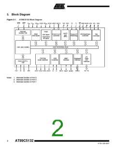
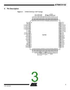
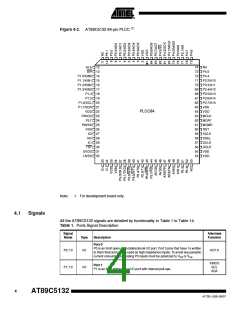
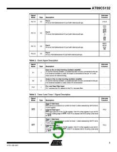
3. Block Diagram
Figure 3-1. AT89C5132 Block Diagram
INT0
1
INT1
1
VDD VSS UVDD UVSS AVDD AVSS AREF AIN1:0 TXD RXD
T0
T1
SS MISO MOSI SCK SCL SDA
1
1
1
1
2
2
2
2
1
1
Interrupt
Handler Unit
Flash
UART
and
BRG
RAM
2304 Bytes
10-bit A-to-D
Converter
Timers 0/1
Watchdog
SPI/DataFlash
Controller
TWI
Controller
64K Bytes
Flash Boot
4K Bytes
8-BIT INTERNAL BUS
C51 (X2 CORE)
I/O
I2S/PCM
Audio Interface
USB
Controller
Keyboard
Interface
Ports
IDE
Interface
MMC
Interface
Clock and PLL
Unit
3
FILT
X1 X2
RST
DOUT DCLK DSEL SCLK D+ D-
MCLK
KIN3:0
P0 - P5
MDAT MCMD
Notes: 1. Alternate function of Port 3
2. Alternate function of Port 4
3. Alternate function of Port 1
2
AT89C5132
4173E–USB–09/07

 ATMEL [ ATMEL ]