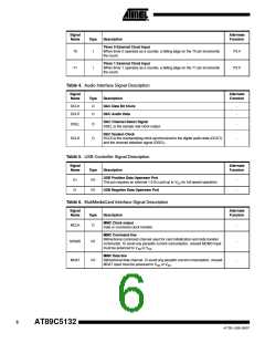
4.2
Internal Pin Structure
Table 15. Detailed Internal Pin Structure
Circuit(1)
Type
Pins
VDD
Input
TST
VDD
Watchdog Output
P
Input/Output
RST
VSS
VDD
VDD
VDD
2 osc
periods
P1(2)
P2(3)
P3
Latch Output
P1
P2
P3
Input/Output
P4
N
P53:0
VSS
VDD
P0
MCMD
MDAT
P
Input/Output
ISP
N
PSEN
VSS
VDD
ALE
SCLK
DCLK
P
Output
DOUT
DSEL
MCLK
N
VSS
D+
D-
Input/Output
D+
D-
Notes: 1. For information on resistors value, input/output levels, and drive capability, refer to the
Section “DC Characteristics”, page 183.
2. When the Two Wire controller is enabled, P1, P2, and P3 transistors are disabled allowing
pseudo open-drain structure.
3. In Port 2, P1 transistor is continuously driven when outputting a high level bit address (A15:8).
10
AT89C5132
4173E–USB–09/07

 ATMEL [ ATMEL ]